SPRAD06B March 2022 – November 2024 AM620-Q1 , AM623 , AM625 , AM625-Q1
- 1
- Abstract
- Trademarks
- 1Overview
-
2DDR4 Board Design and Layout Guidance
- 2.1 DDR4 Introduction
- 2.2 DDR4 Device Implementations Supported
- 2.3 DDR4 Interface Schematics
- 2.4 Compatible JEDEC DDR4 Devices
- 2.5 Placement
- 2.6 DDR4 Keepout Region
- 2.7 DBI
- 2.8 VPP
- 2.9 Net Classes
- 2.10 DDR4 Signal Termination
- 2.11 VREF Routing
- 2.12 VTT
- 2.13 POD Interconnect
- 2.14 CK and ADDR_CTRL Topologies and Routing Guidance
- 2.15 Data Group Topologies and Routing Guidance
- 2.16 CK and ADDR_CTRL Routing Specification
- 2.17 Data Group Routing Specification
- 2.18 Bit Swapping
-
3LPDDR4 Board Design and Layout Guidance
- 3.1 LPDDR4 Introduction
- 3.2 LPDDR4 Device Implementations Supported
- 3.3 LPDDR4 Interface Schematics
- 3.4 Compatible JEDEC LPDDR4 Devices
- 3.5 Placement
- 3.6 LPDDR4 Keepout Region
- 3.7 LPDDR4 DBI
- 3.8 Net Classes
- 3.9 LPDDR4 Signal Termination
- 3.10 LPDDR4 VREF Routing
- 3.11 LPDDR4 VTT
- 3.12 CK0 and ADDR_CTRL Topologies
- 3.13 Data Group Topologies
- 3.14 CK0 and ADDR_CTRL Routing Specification
- 3.15 Data Group Routing Specification
- 3.16 Byte and Bit Swapping
- 4LPDDR4 Board Design Simulations
- 5Appendix: AM62x ALW and AMC Package Delays
- 6Revision History
2.14 CK and ADDR_CTRL Topologies and Routing Guidance
The CK and ADDR_CTRL net classes are routed similarly, and are length matched from the DDR PHY in the processor to each SDRAM to minimize skew between them. The CK net class requires more care because it runs at a higher transition rate and is differential.
The CK and ADDR_CTRL net classes are routed in a ‘fly-by’ implementation. This means that the CK and ADDR_CTRL net classes are routed as a multi-drop bus from the DDR controller in the processor sequentially to each SDRAM, and each signal has a termination at the end. To complete this routing, a small stub trace exists on each net at each SDRAM. These stubs must be short and approximately the same length to manage the reflections. The ADDR_CTRL net class is length matched to the CK net class, at each SDRAM, so that the ADDR_CTRL signals are properly sampled at each SDRAM.
Section 2.2 discussed that there are multiple possible memory topologies, or implementations, ranging from a single x16 SDRAM up to a maximum of two x8 SDRAMs. Regardless of the number of SDRAMs implemented, the routing requirements must be followed. TI recommends that all SDRAMs be implemented on the same side of the board, preferably on the same side of the board as the processor. It is possible to implement the SDRAMs on both sides of the board, but the routing complexity and the number of PCB layers required is significantly increased.
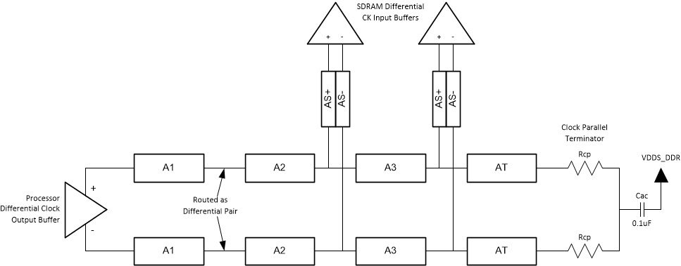
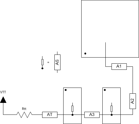
Figure 2-5 shows the topology of the CK net class, and Figure 2-6 shows the topology for the corresponding ADDR_CTRL net class. The fly-by routes have been broken into segments to simplify the length matching analysis. Care must be taken to avoid excessive length error accumulation with this method.
Segments A1 and A2 comprise the lead-in section. Segment AT is the track to the termination at the end of the net. Segments A3 are the routed track between the stubs that branch off to each SDRAM. For topologies with fewer SDRAMs, remove an A3 segment for each SDRAM not present. Length matching requirements for the routing segments are detailed in Table 2-6.
 Figure 2-5 CK Topology for Two DDR4 SDRAM
Devices
 Figure 2-6 ADDR_CTRL Topology for Two
DDR4 SDRAM Devices
Figure 2-6 ADDR_CTRL Topology for Two
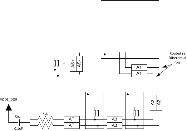
DDR4 SDRAM DevicesThe previous figures show the circuit topology such that the track lengths can be managed and the routed track length matching rules can be followed. The next two figures again show the routing for the CK and ADDR_CTRL routing groups depicted from the perspective of tracks routed on the PCB.
Figure 2-7 shows the CK group routing for two SDRAM devices. The fly-by routing is made clear in this figure. The DDR0_CK0 and DDR0_CK0_n tracks (the CK routing group) are routed as a differential pair from the processor to the SDRAM at the end that will contain BYTE0 data. This differential pair routing then proceeds to the other SDRAM and ends with the AC termination to VDDS_DDR. The routing also includes the routing stubs for both DDR0_CK0 and DDR0_CK0_n at each SDRAM.
 Figure 2-7 CK Routing for Two DDR4 SDRAM
Devices
Figure 2-7 CK Routing for Two DDR4 SDRAM
DevicesFigure 2-8 shows the ADDR_CTRL routing for two SDRAM devices. These are also routed in a fly-by manner along the same path because the ADDR_CTRL routing group is length-matched to the CK routing group.
 Figure 2-8 ADDR_CTRL Routing for Two DDR4
SDRAM Devices
Figure 2-8 ADDR_CTRL Routing for Two DDR4
SDRAM DevicesThe absolute order is not significant. The fly-by routing that starts at the processor can also route down to the SDRAM containing the last byte of data (or whichever SDRAM that is opposite in the row from the one containing the BYTE0 data). The fly-by routing then proceeds to the other SDRAM as discussed above, until it routes to VTT through the Rtt termination after the BYTE0 SDRAM.
Minimize layer transitions during routing. If a layer transition is necessary, it is preferable to transition to a layer using the same reference plane. If this cannot be accommodated, ensure there are nearby stitching vias to allow the return currents to transition between reference planes when both reference planes are ground or VDDS_DDR. Alternately, ensure there are nearby bypass capacitors to allow the return currents to transition between reference planes when one of the reference planes is ground and the other is VDDS_DDR. This must occur at every reference plane transition. The goal is to minimize the size of the return current path thus minimizing the inductance in this path. Lack of these stitching vias or capacitors results in impedance discontinuities in the signal path that increase crosstalk and signal distortion.