SPRAD51A December 2023 – April 2024 F29H850TU , F29H859TU-Q1 , TMS320F2800157 , TMS320F280039 , TMS320F280039-Q1 , TMS320F280039C , TMS320F280039C-Q1 , TMS320F28P659DK-Q1
- 1
- Abstract
- Trademarks
- 1Introduction
- 2Programming Fundamentals
- 3ROM Bootloader and Hex Utility Usage
- 4DCAN Flash Kernel
- 5MCAN Flash Kernel
- 6Example Implementation
- 7Troubleshooting
- 8References
- 9Revision History
6.2.5 Using the Project With CCS
- In CCS, import and build the CPU1 kernel project.
- Launch the target configuration file.
- Connect to CPU1.
- Load the gel file provided in the project folder to the project. Right click on CPU1 in the target configuration and select "Open GEL Files View".
- In the "GEL Files" tab, click on GEL Files. Right click in the "Script" window and select "Load GEL...". Navigate to the project folder and load the gel file.
- In
emulation mode, the following memory locations need to be set to enable CAN boot
mode:
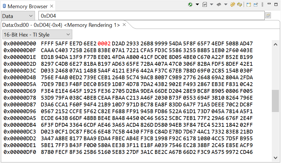
- Location 0xD00 with 0xFFFF
- Location 0xD01 with 0x5AFF
- Location 0xD04 with 0x00XX where XX is the boot mode for CAN Boot – 0x02, 0x22, 0x42 or 0x62. The SENDTEST CAN Boot modes of 0x82, 0xA2, 0xC2 and 0xE2 use the same pins as the first four configurations, respectively, and they also send out two CAN frames. In evaluation mode, using one of the SENDTEST modes ensures that the CAN module does not time out before the host starts sending the flash kernel over. To learn more about the SENDTEST modes, consult the DCAN boot source file located in C2000Ware (C2000Ware_x_xx_xx_xx > driverlib > f28003x > examples > flash > DCAN_Boot.c).
Figure 6-3 shows an example implementation of these memory locations. Once these locations have been programmed, reset the device and click resume. The F28003x device should now be waiting in CAN boot mode in ROM.
 Figure 6-3 Example Memory Window in CCS
(GPIO pins 4/5, CAN Boot Mode)
Figure 6-3 Example Memory Window in CCS
(GPIO pins 4/5, CAN Boot Mode)The PEAK CAN analyzer needs to be connected to the PC as well. No initialization needs to be done beforehand.