SPRAD89 March 2023 AM2631 , AM2631-Q1 , AM2632 , AM2632-Q1 , AM2634 , AM2634-Q1 , AM263P4 , AM263P4-Q1
3.1 Consideration for Proper ADC Sampling
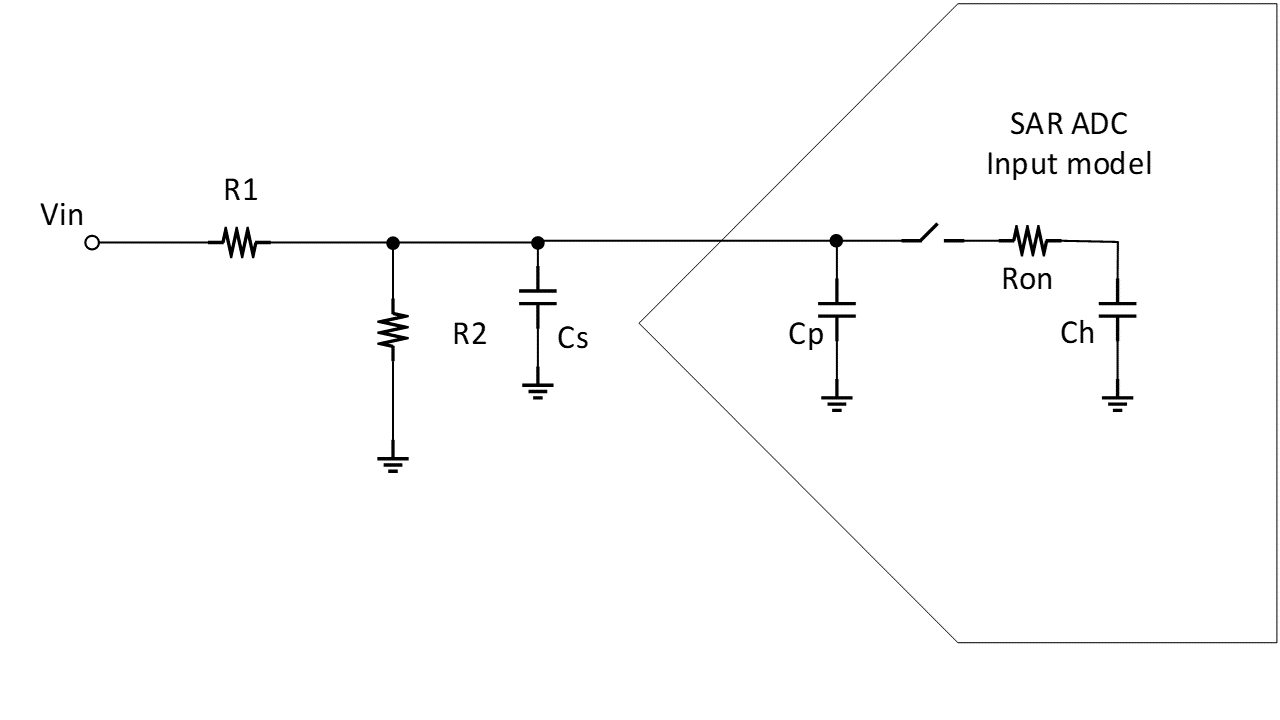
During sampling window, the SAR ADC will have a capacitive network connected to the input and will sample the input voltage. This capacitive network does not provide any resistive loading and hence given enough sampling time, the input will always settle to the correct Vout voltage.

Figure 3-2 ADC Interface
TI’s application note on Charge Sharing Driving Circuits gives an excellent tutorial on how to select source resistors and charge sharing capacitor to drive a SAR ADC.
Cp, Ron, and Ch and sampling time are ADC parameters that are given on the spec sheet of the ADC. Settling error (in LSBs), ADC driving source impedance (Rs = R1//R2) and charge sharing capacitance value (Cs) depend on the application and can be chosen following the guidelines on that application note. Page-30 provides an example on how to select external resistor and capacitor for a voltage divider at the input of a SAR ADC.
As a general guideline, the lower the value of R1, R2 and Cs the faster the response of the network. This guideline should be used for high bandwidth signal paths.