SPRADG4A January   2024  – April 2024


  1.   1
  2.   Abstract
  3.   Trademarks
  4. 1General Texas Instruments High Voltage Evaluation (TI HV EVM) User Safety Guidelines
  5. 2Introduction
  6. 3System Description
    1. 3.1 Key System Specifications
  7. 4System Overview
    1. 4.1 Block Diagram
    2. 4.2 Basic Operation
    3. 4.3 System Design Theory
      1. 4.3.1 Peak Current Mode Control (PCMC) Implementation
      2. 4.3.2 Zero Voltage Switching (ZVS) or Low Voltage Switching (LVS)
      3. 4.3.3 Synchronous Rectification
      4. 4.3.4 Slope Compensation
  8. 5Hardware
    1. 5.1 Hardware Overview
    2. 5.2 Hardware and Test Instruments Required
    3. 5.3 TMDSCNCD263 controlCARD™ Changes
  9. 6Software
    1. 6.1 Getting Started With Firmware
      1. 6.1.1 Opening the Code Composer Studio Project
      2. 6.1.2 Software Architecture
      3. 6.1.3 Project Folder Structure
    2. 6.2 SysConfig Setup
      1. 6.2.1 EPWM Configuration
      2. 6.2.2 ADC Configuration
      3. 6.2.3 CMPSS Configuration
    3. 6.3 Incremental Builds
      1. 6.3.1 Procedure for Running the Incremental Builds - PCMC
        1. 6.3.1.1 Lab 1: Phase Overlapping Check With Open Current and Voltage Loop
          1. 6.3.1.1.1 Objective of Lab 1
          2. 6.3.1.1.2 Overview of Lab 1
          3. 6.3.1.1.3 Procedure of Lab 1
            1. 6.3.1.1.3.1 Start CCS and Open a Project for Lab 1
            2. 6.3.1.1.3.2 Build and Load the Project for Lab 1
            3. 6.3.1.1.3.3 Debug Environment Windows for Lab 1
            4. 6.3.1.1.3.4 Run the Code for Lab 1
        2. 6.3.1.2 Lab 2: Closed Current and Open Voltage Loop
          1. 6.3.1.2.1 Objective of Lab 2
          2. 6.3.1.2.2 Overview of Lab 2
          3. 6.3.1.2.3 Procedure of Lab 2
            1. 6.3.1.2.3.1 Build and Load Project for Lab 2
            2. 6.3.1.2.3.2 Debug Environment Windows for Lab 2
            3. 6.3.1.2.3.3 Run the Code for Lab 2
        3. 6.3.1.3 Lab 3: Closed Current and Closed Voltage Loop
          1. 6.3.1.3.1 Objective of Lab 3
          2. 6.3.1.3.2 Overview of Lab 3
          3. 6.3.1.3.3 Procedure of Lab 3
            1. 6.3.1.3.3.1 Build and Load Project for Lab 3
            2. 6.3.1.3.3.2 Debug Environment Windows for Lab 3
            3. 6.3.1.3.3.3 Run the Code for Lab 3
  10. 7Testing and Results
    1. 7.1 Lab 0: Basic PWM Check
    2. 7.2 Lab 1: Phase Overlapping Check With Open Current and Voltage Loop
    3. 7.3 Lab 2: Closed Current and Open Voltage Loop
    4. 7.4 Lab 3: Closed Current and Closed Voltage Loop
  11. 8References
  12. 9Revision History
Run the Code for Lab 1
  1. Run the code by using the <F8> key, or using the Run button on the toolbar.
  2. Make sure the IO Expander found message is coming in the console as shown in Console message.
  3. Follow the Launch Real Time Debug of AM263x real time Debug guide to enable real time monitoring of the expression window.
  4. Apply an appropriate resistive load to the PSFB system at the DC output. A load that draws around 3A to 6A current at 12V output is a good starting point.
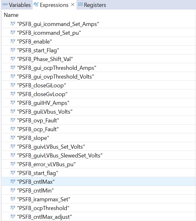
  5. Set PSFB_enable to be 1. This enables PWM output. The expression window is similar to Expression Window.
  6. Power the input at J1, J2 with 300V DC. Observe the PSFB_Phase_Shift_Val parameter in expression window to have a value of 50 at starting (value of 500 indicates 100% phase overlap). Update the value 200. The output is around 6.8V (5A constant current load).
  7. Increase the power input from 300V to 400V. Increase the constant current loading to 12A. Slowly increase PSFB_Phase_Shift_Val to be 300 in incremental steps of 25. Carefully observe the output voltage (PSFB_guiLVbus_Volts), the voltage should gradually increase to 12V. This should not be allowed to exceed the capabilities of the board. Different waveforms, like the PWM gate drive signals, input voltage and current and output voltage can also be probed using an oscilloscope. Appropriate safety precautions should be taken and appropriate grounding requirements should be considered while probing these high voltages and high currents for this isolated DC-DC converter.
  8. Fully stopping the MCU when in real-time mode is a two-step process. With the 400V DC input turned off wait a few seconds. First, stop the processor by using the STOP button on the toolbar. Then turn off the power supply of the MCU.
GUID-4FBB4507-5125-4CE3-91ED-FCE54844EC51-low.png Figure 6-7 Console Message
GUID-E98217D1-A38E-480C-BCB9-2AC4EA075690-low.png Figure 6-8 Expression Window