SPRADG4A January 2024 – April 2024
- 1
- Abstract
- Trademarks
- 1General Texas Instruments High Voltage Evaluation (TI HV EVM) User Safety Guidelines
- 2Introduction
- 3System Description
- 4System Overview
- 5Hardware
-
6Software
- 6.1 Getting Started With Firmware
- 6.2 SysConfig Setup
- 6.3 Incremental Builds
- 7Testing and Results
- 8References
- 9Revision History
4.3.1 Peak Current Mode Control (PCMC) Implementation
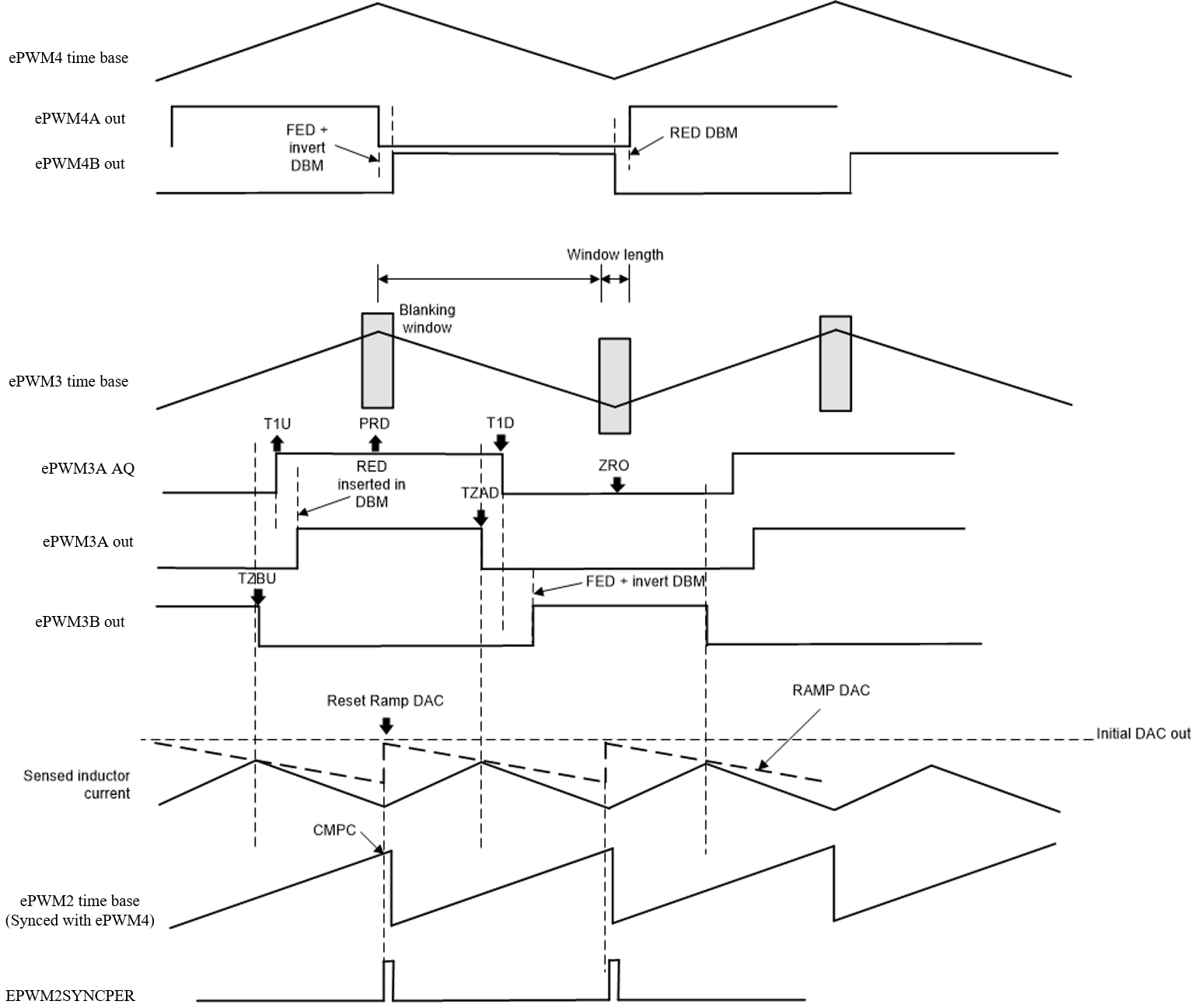
Implementing PCMC for a PSFB system requires complex PWM waveform generation with precise timing control. The Piccolo family of devices from Texas Instruments feature advanced on-chip control peripherals that make this implementation possible without any external support circuitry for this purpose. These peripherals include on-chip analog comparators, digital-to-analog converters (DAC), advanced PWM resources and unique programmable on-chip slope compensation hardware. Figure 4-4 shows the PCMC implementation. Transformer primary current is compared with the peak current reference calculated by the voltage loop using the on-chip comparator.
In every half of the switching cycle when the transformer primary current reaches the commanded peak reference value, one of the PWM waveforms driving the switches (Q2/Q3) is Reset immediately ending the power transfer phase. The PWM waveform driving the other switch in the same leg is Set after a programmable dead-time (dead-band) window. Appropriate slope compensation is also applied that adds a ramp with a programmable negative slope to the peak reference current signal.
The Resetting and Setting action of the PWMs in one leg results in a phase shift between PWM signals driving the two legs. The amount of this phase shift, and thereby the overlap between diagonal switches, is dependent on the amount of peak reference current. Higher the peak reference current, longer the overlap between diagonal switches, and thereby, more the energy transferred to the secondary. The controller regulates the output by controlling this energy transfer by way of controlling the peak reference current value. Thus this peak reference current is the controlled parameter.
An important feature of this implementation is that the same peak reference current command is used for both halves of the switching cycle under all operating conditions. This provides optimal flux balance for the transformer primary reducing any chances of saturation.
 Figure 4-4 PCMC PSFB
Implementation
Figure 4-4 PCMC PSFB
ImplementationThe EPWM4A and EPWM4B outputs are complimentary and 50% duty cycle are maintained based on the action qualifier and deadband settings. The EPWM3A/B_AQ (action qualifier output) is set to 1 when T1U(T1 with counter counting up) event occurs and when counter reaches PRD. The EPWM3A_AQ is set to 0 when T1D (T1 with counter counting down) event occurs and when counter reaches ZERO. The T1D and T1U events are triggered by DCAEVT2.
With type-5 PWM, the deadband can be directly added to T1U and T1D events without adding extra code configurations. The rising edge delay is inserted for EPWM3A. And falling edge delay is inserted for EPWM3B together with inversion accordingly.
To achieve the quickest response, the trip zone modules are utilized to setup the falling edge for EPWM3A (with TZAD event) and EPWM3B (with TZBU event) output. The cycle by cycle trip is implemented and is required to be cleared on ZERO and PRD event.