SPRT766 august 2023 TMS320F28P650DK , TMS320F28P659DK-Q1
|
Key Features and Benefits
|
The F28P65x series is part of the Mid-Performance line of C2000™ real-time microcontroller (MCU) family built for efficient control of power electronics. With an industry leading ultra-low latency, the F28P65x provides further real-time control innovation with more analog, new PWM capabilities while optimizing cost with more integration, and optimized BOM all at the device level. 
Key Applications
|
Addition to the Generation 3 MCU Portfolio
The F28P65x real-time microcontrollers are an extension of the Generation 3 C2000 MCU portfolio. All Generation 3 devices are compatible with C2000WARE software and pin-to-pin compatibility exists between many devices. Figure 1 illustrates the F28P65x series in the portfolio and includes a new focus on application tailored series in the Mid-Performance line.
 Figure 1 C2000 MCU Portfolio With New
F28P65x Mid-Performance Line
Figure 1 C2000 MCU Portfolio With New
F28P65x Mid-Performance LinePin and Packaging Options
The F28P65x MCU series offers two memory and performance configurations and 4 package options with industrial and automotive (-Q1 parts) qualification support. Table 1 provides detailed information about packaging options and key differences.
| Variant | Number of Cores (Running at 200 MHz) | eMHz(1) | Flash | EtherCAT | Lock Step | 100 QFP (16 × 16) |
169 BGA (9 × 9) |
176 QFP (26 × 26) |
256 BGA (13 × 13) |
|---|---|---|---|---|---|---|---|---|---|
| F28P650DK9 | 3 | 1000 | 1.28MB | ✔ | ✔ | ✔ | ✔ | ✔ | |
| F28P650DK8 | 3 | 1000 | 1.28MB | ✔ | ✔ | ✔ | ✔ | ||
| F28P650DK7 | 3 | 1000 | 1.28MB | ✔ | ✔ | ✔ | ✔ | ||
| F28P650SK7 | 2 | 680 | 1.28MB | ✔ | ✔ | ✔ | ✔ | ||
| F28P650DK6 | 3 | 1000 | 1.28MB | ✔ | ✔ | ✔ | ✔ | ||
| F28P650SK6 | 2 | 680 | 1.28MB | ✔ | ✔ | ✔ | ✔ | ||
| F28P650SH7 | 2 | 680 | 768KB | ✔ | ✔ | ✔ | |||
| F28P650DH6 | 3 | 1000 | 768KB | ✔ | |||||
| F28P650SH6 | 2 | 680 | 768KB | ✔ | ✔ | ✔ | |||
| F28P659DK8-Q1 | 3 | 1000 | 1.28MB | ✔ | ✔ | ✔ | ✔ | ||
| F28P659DH8-Q1 | 3 | 1000 | 768KB | ✔ | ✔ | ||||
| F28P659SH6-Q1 | 2 | 680 | 768KB | ✔ | ✔ |
Comparison of Device Features
Compared to other high- and mid-performance devices such as the F2837x and F2838x, the latest addition, F28P65x provides improved precision sensing, advanced actuation with new features, system flexibility and protection, real-time connectivity, advanced safety and security features at an optimized price. Table 2 provides an overview of feature differences between the three.
| Features | F2837x | F2838x | F28P65x |
|---|---|---|---|
| C28x MIPS | Up to 800 | Up to 925 | Up to 600 |
| Number of Cores (running at 200 MHz) |
Up to 4: 2 × C28x CPU + 2 × CLA | Up to 5: 2 × C28x CPU + 2 × CLA + 1 × Cortex M4F | Up to 3: 2 × C28x CPU + 1 × CLA |
| ARM M7 equivalent MHz (eMHz) | 1380 | 1475 | 1000 |
| CLA TMU FPU64 |
2 2 0 |
2 2 2 |
CPU1 – 1; CPU2- 0 2 2 |
| FLASH RAM |
1MB 204KB |
1.5MB 324KB |
1.28MB 248KB |
| PWM | HR | 100 QFP:15ch | 9ch 176 QFP:24ch | 16ch 337 BGA:24ch | 16ch |
176 QFP: 32ch | 16ch 337 BGA: 32ch | 16ch |
100 QFP:36ch | 36ch 169 BGA:36ch | 36ch 176 QFP:36ch | 36ch 256 BGA:36ch | 36ch |
| PWM type | 4 | 4 | 5 |
| ECAP | HR | 6 | 0 | 7 | 2 | 7 | 2 |
| #ADC channels | 100 QFP:14 176 QFP:20 337 BGA:24 |
176 QFP: 20 337 BGA: 24 |
100 QFP: 24 169 BGA: 34 176 QFP: 36 256 BGA: 40 |
| EQEP | 100 QFP:2 176 QFP:3 337 BGA:3 |
176 QFP | 337 BGA:3 | 100 QFP | 169 BGA | 176 QFP | 256 BGA: 6 |
| SDFM | 8 channel | 8 channel | 16 channel |
| CLB | 4 tiles | 8 tiles | 6 tiles |
| FSI | 0-0 | 2Tx-8Rx | 2Tx-4Rx |
| CANFD | 0 | 1 | 2 |
| EtherCAT | 0 | 1 | 1 |
| #GPIO (including AGPIO) | 100 QFP:41 176 QFP:97 337 BGA:169 |
176 QFP:97 337 BGA:169 |
100 QFP: 60 169 BGA: 119 176 QFP: 128 256 BGA: 185 |
| Functional Safety compliant (systematic capability) | SIL-3 | ASIL-D | SIL-3 | ASIL-D | SIL-3 | ASIL-D (target) |
| Security | DCSM | DCSM, Secure boot, JTAG lock, AES | DCSM, Secure boot, JTAG lock, AES |
| Packages | 100QFP,176QFP, 337BGA | 176QFP, 337BGA | 100QFP, 169BGA, 176QFP, 256BGA |
| Starting price 1KU | $7.31 | $10.15 | $5.85 |
Migration From Previous Devices
Customers can successfully design boards to achieve pin to pin compatibility with F2838x and F2837x with the help of the migration guides using the links provided below.
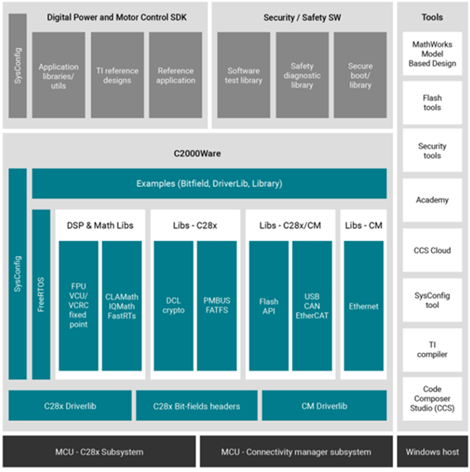
Ecosystem
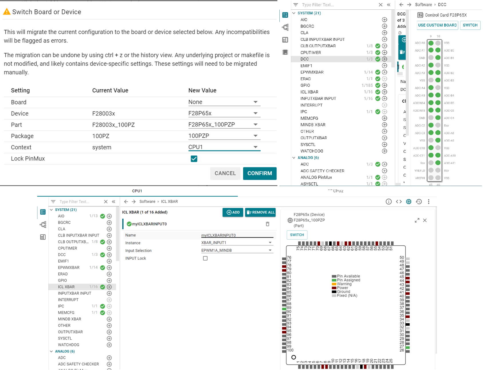
| SysConfig | C2000 SysConfig is a graphical interface tool which
auto-generates content to help designers. The tool is a collection
of information from device TRM, data sheet, errata, migration
guides, application notes, and calculators to make user interface
easier and faster. The C2000 MCU SysConfig offers:
|
 |
||||||
| C2000 Academy and Videos | All available training is
in one place including: getting started resources, interactive
classes, and advanced workshops.
|
|||||||
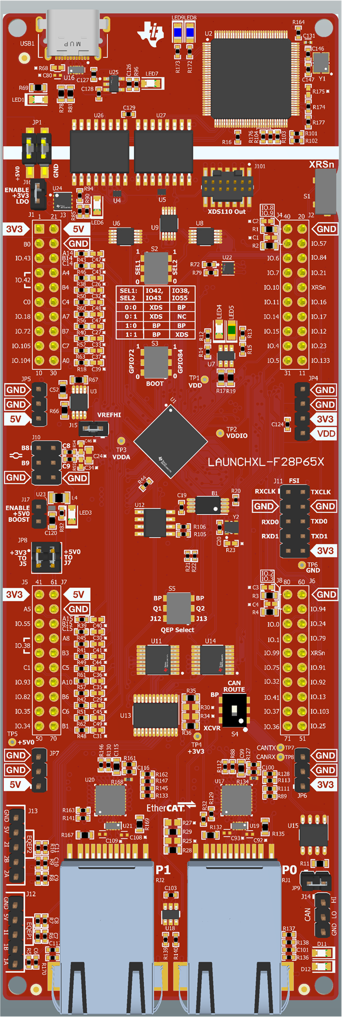
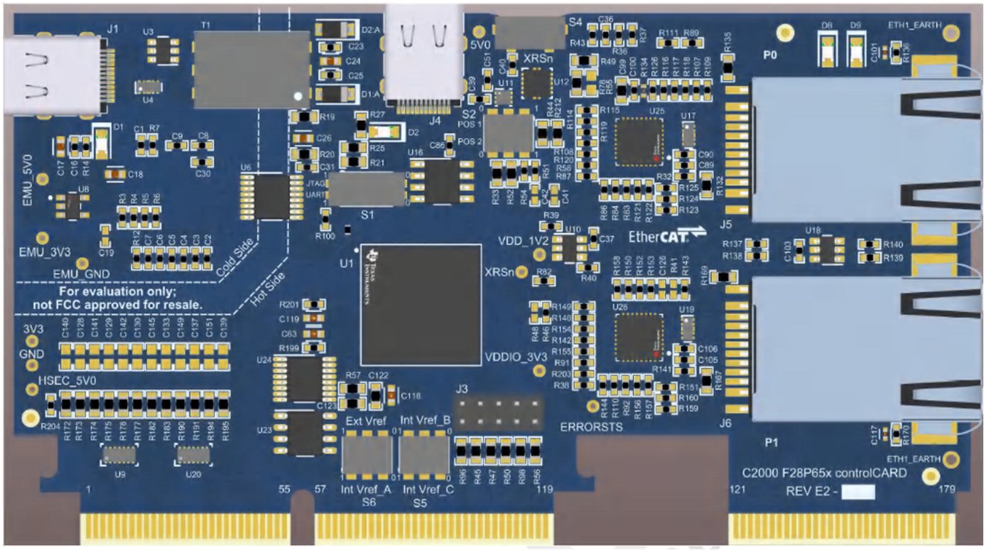
| Software and Hardware |
|
|


