SPRUHZ7K August 2015 – April 2024 AM5706 , AM5708 , AM5716 , AM5718 , AM5718-HIREL
- 1
- Preface
-
1 Introduction
- 1.1 AM571x, AM570x Overview
- 1.2 AM571x, AM570x Environment
- 1.3
AM571x, AM570x Description
- 1.3.1 MPU Subsystem
- 1.3.2 DSP Subsystem
- 1.3.3 PRU-ICSS
- 1.3.4 IPU Subsystems
- 1.3.5 IVA-HD Subsystem
- 1.3.6 Display Subsystem
- 1.3.7 Video Processing Subsystem
- 1.3.8 Video Capture
- 1.3.9 3D GPU Subsystem
- 1.3.10 BB2D Subsystem
- 1.3.11 Camera Interface Subsystem
- 1.3.12 On-Chip Debug Support
- 1.3.13 Power, Reset, and Clock Management
- 1.3.14 On-Chip Memory
- 1.3.15 Memory Management
- 1.3.16 External Memory Interfaces
- 1.3.17 System and Connectivity Peripherals
- 1.4 AM571x, AM570x Family
- 1.5 AM571x, AM570x Device Identification
- 1.6 AM571x, AM570x Package Characteristics Overview
- 2 Memory Mapping
-
3 Power, Reset, and Clock Management
- 3.1
Device Power Management Introduction
- 3.1.1
Device Power-Management Architecture Building Blocks
- 3.1.1.1 Clock Management
- 3.1.1.2 Power Management
- 3.1.1.3 Voltage Management
- 3.1.2 Power-Management Techniques
- 3.1.1
Device Power-Management Architecture Building Blocks
- 3.2 PRCM Subsystem Overview
- 3.3 PRCM Subsystem Environment
- 3.4 PRCM Subsystem Integration
- 3.5
Reset Management Functional Description
- 3.5.1 Overview
- 3.5.2 General Characteristics of Reset Signals
- 3.5.3 Reset Sources
- 3.5.4 Reset Logging
- 3.5.5 Reset Domains
- 3.5.6
Reset Sequences
- 3.5.6.1 MPU Subsystem Power-On Reset Sequence
- 3.5.6.2 MPU Subsystem Warm Reset Sequence
- 3.5.6.3 MPU Subsystem Reset Sequence on Sleep and Wake-Up Transitions From RETENTION State
- 3.5.6.4 IVA Subsystem Power-On Reset Sequence
- 3.5.6.5 IVA Subsystem Software Warm Reset Sequence
- 3.5.6.6 DSP1 Subsystem Power-On Reset Sequence
- 3.5.6.7 DSP1 Subsystem Software Warm Reset Sequence
- 3.5.6.8 IPU1 Subsystem Power-On Reset Sequence
- 3.5.6.9 IPU1 Subsystem Software Warm Reset Sequence
- 3.5.6.10 IPU2 Subsystem Power-On Reset Sequence
- 3.5.6.11 IPU2 Subsystem Software Warm Reset Sequence
- 3.5.6.12 Global Warm Reset Sequence
- 3.6
Clock Management Functional Description
- 3.6.1 Overview
- 3.6.2 External Clock Inputs
- 3.6.3
Internal Clock Sources and Generators
- 3.6.3.1 PRM Clock Source
- 3.6.3.2 CM Clock Source
- 3.6.3.3 Generic DPLL Overview
- 3.6.3.4 DPLL_PER Description
- 3.6.3.5 DPLL_CORE Description
- 3.6.3.6 DPLL_ABE Description
- 3.6.3.7 DPLL_MPU Description
- 3.6.3.8 DPLL_IVA Description
- 3.6.3.9 DPLL_USB Description
- 3.6.3.10 DPLL_DSP Description
- 3.6.3.11 DPLL_GMAC Description
- 3.6.3.12 DPLL_GPU Description
- 3.6.3.13 DPLL_DDR Description
- 3.6.3.14 DPLL_PCIE_REF Description
- 3.6.3.15 APLL_PCIE Description
- 3.6.4
Clock Domains
- 3.6.4.1 CD_WKUPAON Clock Domain
- 3.6.4.2 CD_DSP1 Clock Domain
- 3.6.4.3 CD_CUSTEFUSE Clock Domain
- 3.6.4.4 CD_MPU Clock Domain
- 3.6.4.5 CD_L4PER1 Clock Domain
- 3.6.4.6 CD_L4PER2 Clock Domain
- 3.6.4.7 CD_L4PER3 Clock Domain
- 3.6.4.8 CD_L4SEC Clock Domain
- 3.6.4.9 CD_L3INIT Clock Domain
- 3.6.4.10 CD_IVA Clock Domain
- 3.6.4.11 CD_GPU Description
- 3.6.4.12 CD_EMU Clock Domain
- 3.6.4.13 CD_DSS Clock Domain
- 3.6.4.14 CD_L4_CFG Clock Domain
- 3.6.4.15 CD_L3_INSTR Clock Domain
- 3.6.4.16 CD_L3_MAIN1 Clock Domain
- 3.6.4.17 CD_EMIF Clock Domain
- 3.6.4.18 CD_IPU Clock Domain
- 3.6.4.19 CD_IPU1 Clock Domain
- 3.6.4.20 CD_IPU2 Clock Domain
- 3.6.4.21 CD_DMA Clock Domain
- 3.6.4.22 CD_ATL Clock Domain
- 3.6.4.23 CD_CAM Clock Domain
- 3.6.4.24 CD_GMAC Clock Domain
- 3.6.4.25 CD_VPE Clock Domain
- 3.6.4.26 CD_RTC Clock Domain
- 3.6.4.27 CD_PCIE Clock Domain
- 3.7
Power Management Functional Description
- 3.7.1 PD_WKUPAON Description
- 3.7.2 PD_DSP1 Description
- 3.7.3 PD_CUSTEFUSE Description
- 3.7.4 PD_MPU Description
- 3.7.5 PD_IPU Description
- 3.7.6 PD_L3INIT Description
- 3.7.7 PD_L4PER Description
- 3.7.8 PD_IVA Description
- 3.7.9 PD_GPU Description
- 3.7.10 PD_EMU Description
- 3.7.11 PD_DSS Description
- 3.7.12 PD_CORE Description
- 3.7.13 PD_CAM Description
- 3.7.14 PD_MPUAON Description
- 3.7.15 PD_MMAON Description
- 3.7.16 PD_COREAON Description
- 3.7.17 PD_VPE Description
- 3.7.18 PD_RTC Description
- 3.8 Voltage-Management Functional Description
- 3.9 Device Low-Power States
- 3.10
PRCM Module Programming Guide
- 3.10.1 DPLLs Low-Level Programming Models
- 3.10.2 Clock Management Low-Level Programming Models
- 3.10.3 Power Management Low-Level Programming Models
- 3.11 497
- 3.12 PRCM Software Configuration for OPP_PLUS
- 3.13
PRCM Register Manual
- 3.13.1 Not Supported Functionality (Registers and Bits)
- 3.13.2 PRCM Instance Summary
- 3.13.3 CM_CORE_AON__CKGEN Registers
- 3.13.4 CM_CORE_AON__DSP1 Registers
- 3.13.5 CM_CORE_AON__DSP2 Registers
- 3.13.6 CM_CORE_AON__EVE1 Registers
- 3.13.7 CM_CORE_AON__EVE2 Registers
- 3.13.8 CM_CORE_AON__EVE3 Registers
- 3.13.9 CM_CORE_AON__EVE4 Registers
- 3.13.10 CM_CORE_AON__INSTR Registers
- 3.13.11 CM_CORE_AON__IPU Registers
- 3.13.12 CM_CORE_AON__MPU Registers
- 3.13.13 CM_CORE_AON__OCP_SOCKET Registers
- 3.13.14 CM_CORE_AON__RESTORE Registers
- 3.13.15 CM_CORE_AON__RTC Registers
- 3.13.16 CM_CORE_AON__VPE Registers
- 3.13.17 CM_CORE__CAM Registers
- 3.13.18 CM_CORE__CKGEN Registers
- 3.13.19 CM_CORE__COREAON Registers
- 3.13.20 CM_CORE__CORE Registers
- 3.13.21 CM_CORE__CUSTEFUSE Registers
- 3.13.22 CM_CORE__DSS Registers
- 3.13.23 CM_CORE__GPU Registers
- 3.13.24 CM_CORE__IVA Registers
- 3.13.25 CM_CORE__L3INIT Registers
- 3.13.26 CM_CORE__L4PER Registers
- 3.13.27 CM_CORE__OCP_SOCKET Registers
- 3.13.28 CM_CORE__RESTORE Registers
- 3.13.29 SMARTREFLEX Registers
- 3.13.30 CAM_PRM Registers
- 3.13.31 CKGEN_PRM Registers
- 3.13.32 COREAON_PRM Registers
- 3.13.33 CORE_PRM Registers
- 3.13.34 CUSTEFUSE_PRM Registers
- 3.13.35 DEVICE_PRM Registers
- 3.13.36 DSP1_PRM registers
- 3.13.37 DSP2_PRM Registers
- 3.13.38 DSS_PRM Registers
- 3.13.39 EMU_CM Registers
- 3.13.40 EMU_PRM Registers
- 3.13.41 EVE1_PRM Registers
- 3.13.42 EVE2_PRM Registers
- 3.13.43 EVE3_PRM Registers
- 3.13.44 EVE4_PRM Registers
- 3.13.45 GPU_PRM Registers
- 3.13.46 INSTR_PRM Registers
- 3.13.47 IPU_PRM registers
- 3.13.48 IVA_PRM Registers
- 3.13.49 L3INIT_PRM Registers
- 3.13.50 L4PER_PRM Registers
- 3.13.51 MPU_PRM Registers
- 3.13.52 OCP_SOCKET_PRM Registers
- 3.13.53 RTC_PRM Registers
- 3.13.54 VPE_PRM Registers
- 3.13.55 WKUPAON_CM Registers
- 3.13.56 WKUPAON_PRM registers
- 3.1
Device Power Management Introduction
-
4 Cortex-A15 MPU Subsystem
- 4.1 Cortex-A15 MPU Subsystem Overview
- 4.2 Cortex-A15 MPU Subsystem Integration
- 4.3
Cortex-A15 MPU Subsystem Functional Description
- 4.3.1 MPU Subsystem Block Diagram
- 4.3.2 Cortex-A15 MPCore (MPU_CLUSTER)
- 4.3.3 MPU_AXI2OCP
- 4.3.4 Memory Adapter
- 4.3.5 Realtime Counter (Master Counter)
- 4.3.6 MPU Watchdog Timer
- 4.3.7 MPU Subsystem Power Management
- 4.3.8 MPU Subsystem AMBA Interface Configuration
- 4.4
Cortex-A15 MPU Subsystem Register Manual
- 4.4.1 Cortex-A15 MPU Subsystem Instance Summary
- 4.4.2 MPU_CS_STM Registers
- 4.4.3 MPU_INTC Registers
- 4.4.4 MPU_PRCM_OCP_SOCKET Registers
- 4.4.5 MPU_PRCM_DEVICE Registers
- 4.4.6 MPU_PRCM_PRM_C0 Registers
- 4.4.7 MPU_PRCM_CM_C0 Registers
- 4.4.8 MPU_WUGEN Registers
- 4.4.9 MPU_WD_TIMER Registers
- 4.4.10 MPU_AXI2OCP_MISC Registers
- 4.4.11 MPU_MA_LSM Registers
- 4.4.12 MPU_MA_WP Registers
-
5 DSP Subsystem
- 5.1 DSP Subsystem Overview
- 5.2 DSP Subsystem Integration
- 5.3
DSP Subsystem Functional Description
- 5.3.1 DSP Subsystem Block Diagram
- 5.3.2
DSP Subsystem Components
- 5.3.2.1 C66x DSP Subsystem Introduction
- 5.3.2.2
DSP TMS320C66x CorePac
- 5.3.2.2.1 DSP TMS320C66x CorePac CPU
- 5.3.2.2.2 DSP TMS320C66x CorePac Internal Memory Controllers and Memories
- 5.3.2.2.3
DSP C66x CorePac Internal Peripherals
- 5.3.2.2.3.1 DSP C66x CorePac Interrupt Controller (DSP INTC)
- 5.3.2.2.3.2 DSP C66x CorePac Power-Down Controller (DSP PDC)
- 5.3.2.2.3.3 DSP C66x CorePac Bandwidth Manager (BWM)
- 5.3.2.2.3.4 DSP C66x CorePac Memory Protection Hardware
- 5.3.2.2.3.5 DSP C66x CorePac Internal DMA (IDMA) Controller
- 5.3.2.2.3.6 DSP C66x CorePac External Memory Controller
- 5.3.2.2.3.7 DSP C66x CorePac Extended Memory Controller
- 5.3.2.2.3.8 L1P Memory Error Detection Logic
- 5.3.2.2.3.9 L2 Memory Error Detection and Correction Logic
- 5.3.2.3 DSP Debug and Trace Support
- 5.3.3 DSP System Control Logic
- 5.3.4 DSP Interrupt Requests
- 5.3.5 DSP DMA Requests
- 5.3.6 DSP Intergated Memory Management Units
- 5.3.7 DSP Integrated EDMA Subsystem
- 5.3.8 DSP L2 interconnect Network
- 5.3.9 DSP Boot Configuration
- 5.3.10 DSP Internal and External Memory Views
- 5.4 DSP Subsystem Register Manual
- 6 IVA Subsystem
-
7 Dual Cortex-M4 IPU Subsystem
- 7.1 Dual Cortex-M4 IPU Subsystem Overview
- 7.2 Dual Cortex-M4 IPU Subsystem Integration
- 7.3 Dual Cortex-M4 IPU Subsystem Functional Description
- 7.4 Dual Cortex-M4 IPU Subsystem Register Manual
-
8 Camera Interface Subsystem
- 8.1 CAMSS Overview
- 8.2 CAMSS Environment
- 8.3 CAMSS Integration
- 8.4
CAMSS Functional Description
- 8.4.1 CAMSS Hardware and Software Reset
- 8.4.2 CAMSS Clock Configuration
- 8.4.3 CAMSS Power Management
- 8.4.4 CAMSS Interrupt Events
- 8.4.5 CSI2 PHY Functional Description
- 8.4.6
CAL Functional Description
- 8.4.6.1 CAL Block Diagram
- 8.4.6.2
CSI2 Low Level Protocol
- 8.4.6.2.1 CSI2 Physical Layer
- 8.4.6.2.2 CSI2 Multi-lane Layer and Lane Merger
- 8.4.6.2.3
CSI2 Protocol Layer
- 8.4.6.2.3.1 CSI2 Short Packet
- 8.4.6.2.3.2 CSI2 Long Packet
- 8.4.6.2.3.3 CSI2 ECC and Checksum Generation
- 8.4.6.2.3.4 CSI2 Alignment Constraints
- 8.4.6.2.3.5 CSI2 Data Identifier
- 8.4.6.2.3.6 CSI2 Virtual Channel ID
- 8.4.6.2.3.7 CSI2 Synchronization Codes
- 8.4.6.2.3.8 CSI2 Generic Short Packet Codes
- 8.4.6.2.3.9 CSI2 Frame Structure and Data
- 8.4.6.2.3.10 CSI2 Virtual Channel and Context
- 8.4.6.2.4 CSI2 TAG Generation FSM
- 8.4.6.3 CAL Data Stream Merger
- 8.4.6.4 CAL Pixel Extraction
- 8.4.6.5 CAL DPCM Decoding and Encoding
- 8.4.6.6 CAL Stream Interleaving
- 8.4.6.7 CAL Pixel Packing
- 8.4.6.8 CAL Write DMA
- 8.4.6.9 CAL Video Port
- 8.4.6.10 CAL Registers Shadowing
- 8.5 CAMSS Register Manual
-
9 Video Input Port
- 9.1 VIP Overview
- 9.2 VIP Environment
- 9.3 VIP Integration
- 9.4
VIP Functional Description
- 9.4.1 VIP Block Diagram
- 9.4.2 VIP Software Reset
- 9.4.3 VIP Power and Clocks Management
- 9.4.4
VIP Slice
- 9.4.4.1 VIP Slice Processing Path Overview
- 9.4.4.2 VIP Slice Processing Path Multiplexers
- 9.4.4.3
VIP Slice Processing Path Examples
- 9.4.4.3.1 Input: A=RGB, B=YUV422; Output: A=RGB, B=RGB
- 9.4.4.3.2 Input: A=YUV422 8/16, B=YUV422; Output: A=Scaled YUV420, B=RGB
- 9.4.4.3.3 Input: A=RGB, B=YUV422; Output: A=RGB, B=Scaled YUV420
- 9.4.4.3.4 Input: A=YUV444, B=YUV422; Output: A=YUV422, A=Scaled YUV422, B=YUV422
- 9.4.4.3.5 Input: A=YUV444; Output: A=Scaled YUV420, A=YUV420
- 9.4.4.3.6 Input: A=YUV444; Output: A=Scaled YUV420, A=YUV444
- 9.4.4.3.7 Input: A=YUV422 8/16; Output: A=Scaled YUV420, A=YUV444
- 9.4.4.3.8 Input: A=YUV422 8/16, B=YUV422; Output: A=Scaled YUV420, B=YUV420
- 9.4.4.3.9 Input: A=YUV422 8/16, B=YUV422; Output: A=YUV420, B=YUV420
- 9.4.5
VIP Parser
- 9.4.5.1 Features
- 9.4.5.2 Repacker
- 9.4.5.3 Analog Video
- 9.4.5.4 Digitized Video
- 9.4.5.5 Frame Buffers
- 9.4.5.6
Input Data Interface
- 9.4.5.6.1 8b Interface Mode
- 9.4.5.6.2 16b Interface Mode
- 9.4.5.6.3 24b Interface Mode
- 9.4.5.6.4 Signal Relationships
- 9.4.5.6.5 General 5 Pin Interfaces
- 9.4.5.6.6 Signal Subsets—4 Pin VSYNC, ACTVID, and FID
- 9.4.5.6.7 Signal Subsets—4 Pin VSYNC, HSYNC, and FID
- 9.4.5.6.8 Vertical Sync
- 9.4.5.6.9 Field ID Determination Using Dedicated Signal
- 9.4.5.6.10 Field ID Determination Using VSYNC Skew
- 9.4.5.6.11 Rationale for FID Determination By VSYNC Skew
- 9.4.5.6.12 ACTVID Framing
- 9.4.5.6.13 Ancillary Data Storage in Descrete Sync Mode
- 9.4.5.7 BT.656 Style Embedded Sync
- 9.4.5.8
Source Multiplexing
- 9.4.5.8.1 Multiplexing Scenarios
- 9.4.5.8.2 2-Way Multiplexing
- 9.4.5.8.3 4-Way Multiplexing
- 9.4.5.8.4 Line Multiplexing
- 9.4.5.8.5 Super Frame Concept in Line Multiplexing
- 9.4.5.8.6 8-bit Data Interface in Line Multiplexing
- 9.4.5.8.7 16-bit Data Interface in Line Multiplexing
- 9.4.5.8.8 Split Lines in Line Multiplex Mode
- 9.4.5.8.9 Meta Data
- 9.4.5.8.10 TI Line Mux Mode, Split Lines, and Channel ID Remapping
- 9.4.5.9 Channel ID Extraction for 2x/4x Multiplexed Source
- 9.4.5.10 Embedded Sync Mux Modes and Data Bus Widths
- 9.4.5.11 Ancillary and Active Video Cropping
- 9.4.5.12 Interrupts
- 9.4.5.13 VDET Interrupt
- 9.4.5.14 Source Video Size
- 9.4.5.15 Clipping
- 9.4.5.16 Current and Last FID Value
- 9.4.5.17 Disable Handling
- 9.4.5.18 Picture Size Interrupt
- 9.4.5.19 Discrete Sync Signals
- 9.4.5.20 VIP Overflow Detection and Recovery
- 9.4.6 VIP Color Space Converter (CSC)
- 9.4.7
VIP Scaler (SC)
- 9.4.7.1 SC Features
- 9.4.7.2 SC Functional Description
- 9.4.7.3 SC Code
- 9.4.7.4
SC Coefficient Data Files
- 9.4.7.4.1
HS Polyphase Filter Coefficients
- 9.4.7.4.1.1 ppfcoef_scale_eq_1_32_phases_flip.dat
- 9.4.7.4.1.2 ppfcoef_scale_eq_8div16_32_phases_flip.dat
- 9.4.7.4.1.3 ppfcoef_scale_eq_9div16_32_phases_flip.dat
- 9.4.7.4.1.4 ppfcoef_scale_eq_10div16_32_phases_flip.dat
- 9.4.7.4.1.5 ppfcoef_scale_eq_11div16_32_phases_flip.dat
- 9.4.7.4.1.6 ppfcoef_scale_eq_12div16_32_phases_flip.dat
- 9.4.7.4.1.7 ppfcoef_scale_eq_13div16_32_phases_flip.dat
- 9.4.7.4.1.8 ppfcoef_scale_eq_14div16_32_phases_flip.dat
- 9.4.7.4.1.9 ppfcoef_scale_eq_15div16_32_phases_flip.dat
- 9.4.7.4.2
VS Polyphase Filter Coefficients
- 9.4.7.4.2.1 ppfcoef_scale_eq_1_32_phases_ver_5tap_flip.dat
- 9.4.7.4.2.2 ppfcoef_scale_eq_3_32_phases_flip.dat
- 9.4.7.4.2.3 ppfcoef_scale_eq_4_32_phases_flip.dat
- 9.4.7.4.2.4 ppfcoef_scale_eq_5_32_phases_flip.dat
- 9.4.7.4.2.5 ppfcoef_scale_eq_6_32_phases_flip.dat
- 9.4.7.4.2.6
ppfcoef_scale_eq_7_32_phases_flip.dat
- 9.4.7.4.2.6.1 ppfcoef_scale_eq_8div16_32_phases_ver_5tap_flip.dat
- 9.4.7.4.2.6.2 ppfcoef_scale_eq_9div16_32_phases_ver_5tap_flip.dat
- 9.4.7.4.2.6.3 ppfcoef_scale_eq_10div16_32_phases_ver_5tap_flip.dat
- 9.4.7.4.2.6.4 ppfcoef_scale_eq_11div16_32_phases_ver_5tap_flip.dat
- 9.4.7.4.2.6.5 ppfcoef_scale_eq_12div16_32_phases_ver_5tap_flip.dat
- 9.4.7.4.2.6.6 ppfcoef_scale_eq_13div16_32_phases_ver_5tap_flip.dat
- 9.4.7.4.2.6.7 ppfcoef_scale_eq_14div16_32_phases_ver_5tap_flip.dat
- 9.4.7.4.2.6.8 ppfcoef_scale_eq_15div16_32_phases_ver_5tap_flip.dat
- 9.4.7.4.3 VS (Bilinear Filter Coefficients)
- 9.4.7.4.1
HS Polyphase Filter Coefficients
- 9.4.8
VIP Video Port Direct Memory Access (VPDMA)
- 9.4.8.1 VPDMA Introduction
- 9.4.8.2 VPDMA Basic Definitions
- 9.4.8.3 1107
- 9.4.8.4 VPDMA Client Buffering and Functionality
- 9.4.8.5 VPDMA Channels Assignment
- 9.4.8.6 VPDMA MFLAG Mechanism
- 9.4.8.7 VPDMA Interrupts
- 9.4.8.8
VPDMA Descriptors
- 9.4.8.8.1 Data Transfer Descriptors
- 9.4.8.8.2 Configuration Descriptor
- 9.4.8.8.3 Control Descriptor
- 9.4.8.9 VPDMA Configuration
- 9.4.8.10
VPDMA Data Formats
- 9.4.8.10.1
YUV Data Formats
- 9.4.8.10.1.1 Y 4:4:4 (Data Type 0)
- 9.4.8.10.1.2 Y 4:2:2 (Data Type 1)
- 9.4.8.10.1.3 Y 4:2:0 (Data Type 2)
- 9.4.8.10.1.4 C 4:4:4 (Data Type 4)
- 9.4.8.10.1.5 C 4:2:2 (Data Type 5)
- 9.4.8.10.1.6 C 4:2:0 (Data Type 6)
- 9.4.8.10.1.7 YC 4:2:2 (Data Type 7)
- 9.4.8.10.1.8 YC 4:4:4 (Data Type 8)
- 9.4.8.10.1.9 CY 4:2:2 (Data Type 23)
- 9.4.8.10.2
RGB Data Formats
- 9.4.8.10.2.1 RGB16-565 (Data Type 0)
- 9.4.8.10.2.2 ARGB-1555 (Data Type 1)
- 9.4.8.10.2.3 ARGB-4444 (Data Type 2)
- 9.4.8.10.2.4 RGBA-5551 (Data Type 3)
- 9.4.8.10.2.5 RGBA-4444 (Data Type 4)
- 9.4.8.10.2.6 ARGB24-6666 (Data Type 5)
- 9.4.8.10.2.7 RGB24-888 (Data Type 6)
- 9.4.8.10.2.8 ARGB32-8888 (Data Type 7)
- 9.4.8.10.2.9 RGBA24-6666 (Data Type 8)
- 9.4.8.10.2.10 RGBA32-8888 (Data Type 9)
- 9.4.8.10.3 Miscellaneous Data Type
- 9.4.8.10.1
YUV Data Formats
- 9.5 VIP Register Manual
-
10Video Processing Engine
- 10.1 VPE Overview
- 10.2 VPE Integration
- 10.3
VPE Functional Description
- 10.3.1 VPE Block Diagram
- 10.3.2 VPE VC1 Range Mapping/Range Reduction
- 10.3.3 VPE Deinterlacer (DEI)
- 10.3.4
VPE Scaler (SC)
- 10.3.4.1 SC Features
- 10.3.4.2 SC Functional Description
- 10.3.4.3 SC Code
- 10.3.4.4
SC Coefficient Data Files
- 10.3.4.4.1
HS Polyphase Filter Coefficients
- 10.3.4.4.1.1 ppfcoef_scale_eq_1_32_phases_flip.dat
- 10.3.4.4.1.2 ppfcoef_scale_eq_8div16_32_phases_flip.dat
- 10.3.4.4.1.3 ppfcoef_scale_eq_9div16_32_phases_flip.dat
- 10.3.4.4.1.4 ppfcoef_scale_eq_10div16_32_phases_flip.dat
- 10.3.4.4.1.5 ppfcoef_scale_eq_11div16_32_phases_flip.dat
- 10.3.4.4.1.6 ppfcoef_scale_eq_12div16_32_phases_flip.dat
- 10.3.4.4.1.7 ppfcoef_scale_eq_13div16_32_phases_flip.dat
- 10.3.4.4.1.8 ppfcoef_scale_eq_14div16_32_phases_flip.dat
- 10.3.4.4.1.9 ppfcoef_scale_eq_15div16_32_phases_flip.dat
- 10.3.4.4.2
VS Polyphase Filter Coefficients
- 10.3.4.4.2.1 ppfcoef_scale_eq_1_32_phases_ver_5tap_flip.dat
- 10.3.4.4.2.2 ppfcoef_scale_eq_3_32_phases_flip.dat
- 10.3.4.4.2.3 ppfcoef_scale_eq_4_32_phases_flip.dat
- 10.3.4.4.2.4 ppfcoef_scale_eq_5_32_phases_flip.dat
- 10.3.4.4.2.5 ppfcoef_scale_eq_6_32_phases_flip.dat
- 10.3.4.4.2.6
ppfcoef_scale_eq_7_32_phases_flip.dat
- 10.3.4.4.2.6.1 ppfcoef_scale_eq_8div16_32_phases_ver_5tap_flip.dat
- 10.3.4.4.2.6.2 ppfcoef_scale_eq_9div16_32_phases_ver_5tap_flip.dat
- 10.3.4.4.2.6.3 ppfcoef_scale_eq_10div16_32_phases_ver_5tap_flip.dat
- 10.3.4.4.2.6.4 ppfcoef_scale_eq_11div16_32_phases_ver_5tap_flip.dat
- 10.3.4.4.2.6.5 ppfcoef_scale_eq_12div16_32_phases_ver_5tap_flip.dat
- 10.3.4.4.2.6.6 ppfcoef_scale_eq_13div16_32_phases_ver_5tap_flip.dat
- 10.3.4.4.2.6.7 ppfcoef_scale_eq_14div16_32_phases_ver_5tap_flip.dat
- 10.3.4.4.2.6.8 ppfcoef_scale_eq_15div16_32_phases_ver_5tap_flip.dat
- 10.3.4.4.2.6.9 ppcoef_scale_1x_ver_5tap.dat
- 10.3.4.4.3 VS (Bilinear Filter Coefficients)
- 10.3.4.4.1
HS Polyphase Filter Coefficients
- 10.3.5 VPE Color Space Converter (CSC)
- 10.3.6 VPE Chroma Up-Sampler (CHR_US)
- 10.3.7 VPE Chroma Down-Sampler (CHR_DS)
- 10.3.8 VPE YUV422 to YUV444 Conversion
- 10.3.9
VPE Video Port Direct Memory Access (VPDMA)
- 10.3.9.1 VPDMA Introduction
- 10.3.9.2 VPDMA Basic Definitions
- 10.3.9.3 VPDMA Client Buffering and Functionality
- 10.3.9.4 VPDMA Channels Assignment
- 10.3.9.5 VPDMA Interrupts
- 10.3.9.6
VPDMA Descriptors
- 10.3.9.6.1
Data Transfer Descriptors
- 10.3.9.6.1.1 Data Packet Descriptor Word 0 (Data)
- 10.3.9.6.1.2 Data Packet Descriptor Word 1
- 10.3.9.6.1.3 Data Packet Descriptor Word 2
- 10.3.9.6.1.4 Data Packet Descriptor Word 3
- 10.3.9.6.1.5 Data Packet Descriptor Word 4
- 10.3.9.6.1.6 Data Packet Descriptor Word 5
- 10.3.9.6.1.7 Data Packet Descriptor Word 6/7 (Data)
- 10.3.9.6.2 Configuration Descriptor
- 10.3.9.6.3 Control Descriptor
- 10.3.9.6.1
Data Transfer Descriptors
- 10.3.9.7 VPDMA Configuration
- 10.3.9.8
VPDMA Data Formats
- 10.3.9.8.1
YUV Data Formats
- 10.3.9.8.1.1 Y 4:4:4 (Data Type 0)
- 10.3.9.8.1.2 Y 4:2:2 (Data Type 1)
- 10.3.9.8.1.3 Y 4:2:0 (Data Type 2)
- 10.3.9.8.1.4 C 4:4:4 (Data Type 4)
- 10.3.9.8.1.5 C 4:2:2 (Data Type 5)
- 10.3.9.8.1.6 C 4:2:0 (Data Type 6)
- 10.3.9.8.1.7 YC 4:2:2 (Data Type 7)
- 10.3.9.8.1.8 YC 4:4:4 (Data Type 8)
- 10.3.9.8.1.9 CY 4:2:2 (Data Type 23)
- 10.3.9.8.2
RGB Data Formats
- 10.3.9.8.2.1
Input Data Formats
- 10.3.9.8.2.1.1 RGB16-565 (Data Type 0)
- 10.3.9.8.2.1.2 ARGB-1555 (Data Type 1)
- 10.3.9.8.2.1.3 ARGB-4444 (Data Type 2)
- 10.3.9.8.2.1.4 RGBA-5551 (Data Type 3)
- 10.3.9.8.2.1.5 RGBA-4444 (Data Type 4)
- 10.3.9.8.2.1.6 ARGB24-6666 (Data Type 5)
- 10.3.9.8.2.1.7 RGB24-888 (Data Type 6)
- 10.3.9.8.2.1.8 ARGB32-8888 (Data Type 7)
- 10.3.9.8.2.1.9 RGBA24-6666 (Data Type 8)
- 10.3.9.8.2.1.10 RGBA32-8888 (Data Type 9)
- 10.3.9.8.2.2
Output Data Formats
- 10.3.9.8.2.2.1 RGB16-565 (Data Type 0)
- 10.3.9.8.2.2.2 ARGB-1555 (Data Type 1)
- 10.3.9.8.2.2.3 ARGB-4444 (Data Type 2)
- 10.3.9.8.2.2.4 RGBA-5551 (Data Type 3)
- 10.3.9.8.2.2.5 RGBA-4444 (Data Type 4)
- 10.3.9.8.2.2.6 ARGB24-6666 (Data Type 5)
- 10.3.9.8.2.2.7 RGB24-888 (Data Type 6)
- 10.3.9.8.2.2.8 ARGB32-8888 (Data Type 7)
- 10.3.9.8.2.2.9 RGBA24-6666 (Data Type 8)
- 10.3.9.8.2.2.10 RGBA32-8888 (Data Type 9)
- 10.3.9.8.2.1
Input Data Formats
- 10.3.9.8.3 Miscellaneous Data Type
- 10.3.9.8.1
YUV Data Formats
- 10.3.10 VPE Software Reset
- 10.3.11 VPE Power and Clocks Management
- 10.4 VPE Register Manual
-
11Display Subsystem
- 11.1
Display Subsystem Overview
- 11.1.1 Display Subsystem Environment
- 11.1.2 Display Subsystem Integration
- 11.1.3
Display Subsystem DPLL Controllers Functional Description
- 11.1.3.1 DPLL Controllers Overview
- 11.1.3.2 OCP2SCP2 Functional Description
- 11.1.3.3
DPLL_VIDEO Functional Description
- 11.1.3.3.1 DPLL_VIDEO Controller Architecture
- 11.1.3.3.2 DPLL_VIDEO Operations
- 11.1.3.3.3 DPLL_VIDEO Error Handling
- 11.1.3.3.4 DPLL_VIDEO Software Reset
- 11.1.3.3.5 DPLL_VIDEO Power Management
- 11.1.3.3.6 DPLL_VIDEO HSDIVIDER Loading Operation
- 11.1.3.3.7 DPLL_VIDEO Clock Sequence
- 11.1.3.3.8 DPLL_VIDEO Go Sequence
- 11.1.3.3.9 DPLL_VIDEO Recommended Values
- 11.1.3.4
DPLL_HDMI Functional Description
- 11.1.3.4.1 DPLL_HDMI and PLLCTRL_HDMI Overview
- 11.1.3.4.2 DPLL_HDMI and PLLCTRL_HDMI Architecture
- 11.1.3.4.3 DPLL_HDMI Operations
- 11.1.3.4.4 DPLL_HDMI Register Access
- 11.1.3.4.5 DPLL_HDMI Error Handling
- 11.1.3.4.6 DPLL_HDMI Software Reset
- 11.1.3.4.7 DPLL_HDMI Power Management
- 11.1.3.4.8 DPLL_HDMI Lock Sequence
- 11.1.3.4.9 DPLL_HDMI Go Sequence
- 11.1.3.4.10 DPLL_HDMI Recommended Values
- 11.1.4 Display Subsystem Programming Guide
- 11.1.5 Display Subsystem Register Manual
- 11.2
Display Controller
- 11.2.1 DISPC Overview
- 11.2.2 DISPC Environment
- 11.2.3 DISPC Integration
- 11.2.4
DISPC Functional Description
- 11.2.4.1 DISPC Clock Configuration
- 11.2.4.2 DISPC Software Reset
- 11.2.4.3 DISPC Power Management
- 11.2.4.4 DISPC Interrupt Requests
- 11.2.4.5 DISPC DMA Requests
- 11.2.4.6
DISPC DMA Engine
- 11.2.4.6.1 DISPC Addressing and Bursts
- 11.2.4.6.2 DISPC Immediate Base Address Flip Mechanism
- 11.2.4.6.3 DISPC DMA Buffers
- 11.2.4.6.4 DISPC MFLAG Mechanism and Arbitration
- 11.2.4.6.5 DISPC Predecimation
- 11.2.4.6.6 DISPC Progressive-to-Interlaced Format Conversion
- 11.2.4.6.7 DISPC Arbitration
- 11.2.4.6.8 DISPC DMA Power Modes
- 11.2.4.7 DISPC Rotation and Mirroring
- 11.2.4.8 DISPC Memory Format
- 11.2.4.9 DISPC Graphics Pipeline
- 11.2.4.10 DISPC Video Pipelines
- 11.2.4.11 DISPC Write-Back Pipeline
- 11.2.4.12 DISPC Hardware Cursor
- 11.2.4.13
DISPC LCD Outputs
- 11.2.4.13.1 DISPC Overlay Manager
- 11.2.4.13.2 DISPC Gamma Correction Unit
- 11.2.4.13.3 DISPC Color Phase Rotation Unit
- 11.2.4.13.4 DISPC Color Space Conversion
- 11.2.4.13.5 DISPC BT.656 and BT.1120 Modes
- 11.2.4.13.6 DISPC Active Matrix
- 11.2.4.13.7 DISPC Synchronized Buffer Update
- 11.2.4.13.8 DISPC Timing Generator and Panel Settings
- 11.2.4.14 DISPC TV Output
- 11.2.4.15 DISPC Frame Width Considerations
- 11.2.4.16 DISPC Extended 3D Support
- 11.2.4.17 DISPC Shadow Registers
- 11.2.5
DISPC Programming Guide
- 11.2.5.1
DISPC Low-Level Programming Models
- 11.2.5.1.1 DISPC Global Initialization
- 11.2.5.1.2
DISPC Operational Modes Configuration
- 11.2.5.1.2.1 DISPC DMA Configuration
- 11.2.5.1.2.2 DISPC GFX Pipeline Configuration
- 11.2.5.1.2.3
DISPC Video Pipeline Configuration
- 11.2.5.1.2.3.1 DISPC Main Sequence – Configure the Video Pipeline
- 11.2.5.1.2.3.2 DISPC Subsequence – Configure the Video Window
- 11.2.5.1.2.3.3 DISPC Subsequence – Configure the Video Pipeline Processing
- 11.2.5.1.2.3.4 DISPC Subsequence – Configure the VC-1 Range Mapping
- 11.2.5.1.2.3.5 DISPC Subsequence – Configure the Video Color Space Conversion
- 11.2.5.1.2.3.6 DISPC Subsequence – Configure the Video Scaler Unit
- 11.2.5.1.2.3.7 DISPC Subsequence – Configure the Video Pipeline Layer Output
- 11.2.5.1.2.4 DISPC WB Pipeline Configuration
- 11.2.5.1.2.5
DISPC LCD Output Configuration
- 11.2.5.1.2.5.1 DISPC Main Sequence – Configure the LCD Output
- 11.2.5.1.2.5.2 DISPC Subsequence – Configure the Overlay Manager
- 11.2.5.1.2.5.3 DISPC Subsequence – Configure the Gamma Table for Gamma Correction
- 11.2.5.1.2.5.4 DISPC Subsequence – Configure the Color Phase Rotation
- 11.2.5.1.2.5.5 DISPC Subsequence – Configure the LCD Panel Timings and Parameters
- 11.2.5.1.2.5.6 DISPC Subsequence – Configure BT.656 or BT.1120 Mode
- 11.2.5.1.2.6 DISPC TV Output Configuration
- 11.2.5.1
DISPC Low-Level Programming Models
- 11.2.6 DISPC Register Manual
- 11.3 High-Definition Multimedia Interface
- 11.1
Display Subsystem Overview
- 123D Graphics Accelerator
- 132D Graphics Accelerator
-
14Interconnect
- 14.1 Interconnect Overview
- 14.2
L3_MAIN Interconnect
- 14.2.1 L3_MAIN Interconnect Overview
- 14.2.2 L3_MAIN Interconnect Integration
- 14.2.3
L3_MAIN Interconnect Functional Description
- 14.2.3.1 Module Use in L3_MAIN Interconnect
- 14.2.3.2 Module Distribution
- 14.2.3.3 Bandwidth Regulators
- 14.2.3.4 Bandwidth Limiters
- 14.2.3.5 Flag Muxing
- 14.2.3.6 Statistic Collectors Group
- 14.2.3.7 L3_MAIN Protection and Firewalls
- 14.2.3.8 L3_MAIN Interconnect Error Handling
- 14.2.4
L3_MAIN Interconnect Programming Guide
- 14.2.4.1 L3 _MAIN Interconnect Low-Level Programming Models
- 14.2.4.2
Operational Modes Configuration
- 14.2.4.2.1
L3_MAIN Interconnect Error Analysis Mode
- 14.2.4.2.1.1
Main Sequence: L3_MAIN Interconnect Error Analysis Mode
- 14.2.4.2.1.1.1 Subsequence: L3_MAIN Custom Error Identification
- 14.2.4.2.1.1.2 Subsequence: L3_MAIN Interconnect Protection Violation Error Identification
- 14.2.4.2.1.1.3 Subsequence: L3_MAIN Interconnect Standard Error Identification
- 14.2.4.2.1.1.4 Subsequence: L3_MAIN Interconnect FLAGMUX Configuration
- 14.2.4.2.1.1
Main Sequence: L3_MAIN Interconnect Error Analysis Mode
- 14.2.4.2.1
L3_MAIN Interconnect Error Analysis Mode
- 14.2.5
L3_MAIN Interconnect Register Manual
- 14.2.5.1
L3_MAIN Register Group Summary
- 14.2.5.1.1 L3_MAIN Firewall Registers Summary and Description
- 14.2.5.1.2 L3_MAIN Host Register Summary and Description
- 14.2.5.1.3 L3_MAIN TARG Register Summary and Description
- 14.2.5.1.4 L3_MAIN FLAGMUX Registers Summary and Description
- 14.2.5.1.5 L3_MAIN FLAGMUX CLK1MERGE Registers Summary and Description
- 14.2.5.1.6 L3_MAIN FLAGMUX TIMEOUT Registers Summary and Description
- 14.2.5.1.7 L3_MAIN BW Regulator Register Summary and Description
- 14.2.5.1.8 L3_MAIN Bandwidth Limiter Register Summary and Description
- 14.2.5.1.9 L3_MAIN STATCOLL Register Summary and Description
- 14.2.5.1
L3_MAIN Register Group Summary
- 14.3
L4 Interconnects
- 14.3.1 L4 Interconnect Overview
- 14.3.2 L4 Interconnect Integration
- 14.3.3 L4 Interconnect Functional Description
- 14.3.4
L4 Interconnect Programming Guide
- 14.3.4.1
L4 Interconnect Low-level Programming Models
- 14.3.4.1.1 Global Initialization
- 14.3.4.1.2
Operational Modes Configuration
- 14.3.4.1.2.1
L4 Interconnect Error Analysis Mode
- 14.3.4.1.2.1.1 Main Sequence: L4 Interconnect Error Analysis Mode
- 14.3.4.1.2.1.2 Subsequence: L4 Interconnect Protection Violation Error Identification
- 14.3.4.1.2.1.3 Subsequence: L4 Interconnect Unsupported Command/Address Hole Error Identification
- 14.3.4.1.2.1.4 Subsequence: L4 Interconnect Reset TA and Module
- 14.3.4.1.2.2 L4 Interconnect Time-Out Configuration Mode
- 14.3.4.1.2.3 L4 Interconnect Firewall Configuration Mode
- 14.3.4.1.2.1
L4 Interconnect Error Analysis Mode
- 14.3.4.1
L4 Interconnect Low-level Programming Models
- 14.3.5 L4 Interconnects Register Manual
-
15Memory Subsystem
- 15.1 Memory Subsystem Overview
- 15.2
Dynamic Memory Manager
- 15.2.1 DMM Overview
- 15.2.2 DMM Integration
- 15.2.3
DMM Functional Description
- 15.2.3.1 DMM Block Diagram
- 15.2.3.2 DMM Clock Configuration
- 15.2.3.3 DMM Power Management
- 15.2.3.4 DMM Interrupt Requests
- 15.2.3.5 DMM
- 15.2.3.6
TILER
- 15.2.3.6.1
TILER Concepts
- 15.2.3.6.1.1
TILER Rationale
- 15.2.3.6.1.1.1 The TILER is a 4-GiB Virtual Address Space Composed of Eight Views
- 15.2.3.6.1.1.2 A View is a 512-MiB Virtual Address Space Composed of Four Containers
- 15.2.3.6.1.1.3 A Container is a 128-MiB Virtual Address Space
- 15.2.3.6.1.1.4 A Page is a 4-kiB Virtual Address Space
- 15.2.3.6.1.1.5 A Tile is a 1-kiB Address Space
- 15.2.3.6.1.1.6 1851
- 15.2.3.6.1.1.7 A Subtile is a 128-Bit Address Space
- 15.2.3.6.1.2 TILER Modes
- 15.2.3.6.1.3 Object Container Definition
- 15.2.3.6.1.4 Page Definition
- 15.2.3.6.1.5 Orientation
- 15.2.3.6.1.6 Tile Definition
- 15.2.3.6.1.7 Subtiles
- 15.2.3.6.1.8
TILER Virtual Addressing
- 15.2.3.6.1.8.1 Page Mode Virtual Addressing and Characteristics
- 15.2.3.6.1.8.2 Tiled Mode Virtual Addressing and Characteristics
- 15.2.3.6.1.8.3
Element Ordering in the TILER Container
- 15.2.3.6.1.8.3.1 Natural View or 0-Degree View (Orientation 0)
- 15.2.3.6.1.8.3.2 0-Degree View With Vertical Mirror or 180-Degree View With Horizontal Mirror (Orientation 1)
- 15.2.3.6.1.8.3.3 0-Degree View With Horizontal Mirror or 180-Degree View With Vertical Mirror (Orientation 2)
- 15.2.3.6.1.8.3.4 180-Degree View (Orientation 3)
- 15.2.3.6.1.8.3.5 90-Degree View With Vertical Mirror or 270-Degree View With Horizontal Mirror (Orientation 4)
- 15.2.3.6.1.8.3.6 270-Degree View (Orientation 5)
- 15.2.3.6.1.8.3.7 90-Degree View (Orientation 6)
- 15.2.3.6.1.8.3.8 90-Degree View With Horizontal Mirror or 270-Degree View With Vertical Mirror (Orientation 7)
- 15.2.3.6.1.1
TILER Rationale
- 15.2.3.6.2 TILER Macro-Architecture
- 15.2.3.6.3 TILER Guidelines for Initiators
- 15.2.3.6.1
TILER Concepts
- 15.2.4 DMM Use Cases and Tips
- 15.2.5
DMM Basic Programming Model
- 15.2.5.1 Global Initialization
- 15.2.5.2 DMM Module Global Initialization
- 15.2.5.3 DMM Operational Modes Configuration
- 15.2.5.4 Addressing an Object in Tiled Mode
- 15.2.5.5 Addressing an Object in Page Mode
- 15.2.5.6 Sharing Containers Between Different Modes
- 15.2.6 DMM Register Manual
- 15.3
EMIF Controller
- 15.3.1 EMIF Controller Overview
- 15.3.2 EMIF Module Environment
- 15.3.3 EMIF Module Integration
- 15.3.4
EMIF Functional Description
- 15.3.4.1 Block Diagram
- 15.3.4.2 Clock Management
- 15.3.4.3 Reset
- 15.3.4.4 System Power Management
- 15.3.4.5 Interrupt Requests
- 15.3.4.6 SDRAM Refresh Scheduling
- 15.3.4.7 SDRAM Initialization
- 15.3.4.8 DDR3/DDR3L Read-Write Leveling
- 15.3.4.9 EMIF Access Cycles
- 15.3.4.10 Turnaround Time
- 15.3.4.11 PHY DLL Calibration
- 15.3.4.12
SDRAM Address Mapping
- 15.3.4.12.1 Address Mapping for IBANK_POS = 0 and EBANK_POS = 0
- 15.3.4.12.2 Address Mapping for IBANK_POS = 1 and EBANK_POS = 0
- 15.3.4.12.3 Address Mapping for IBANK_POS = 2 and EBANK_POS = 0
- 15.3.4.12.4 Address Mapping for IBANK_POS = 3 and EBANK_POS = 0
- 15.3.4.12.5 Address Mapping for IBANK_POS = 0 and EBANK_POS = 1
- 15.3.4.12.6 Address Mapping for IBANK_POS = 1 and EBANK_POS = 1
- 15.3.4.12.7 Address Mapping for IBANK_POS = 2 and EBANK_POS = 1
- 15.3.4.12.8 1949
- 15.3.4.12.9 Address Mapping for IBANK_POS = 3 and EBANK_POS = 1
- 15.3.4.12.10 1951
- 15.3.4.13 DDR3/DDR3L Output Impedance Calibration
- 15.3.4.14 Error Correction And Detection Feature
- 15.3.4.15 Class of Service
- 15.3.4.16 Performance Counters
- 15.3.4.17 Forcing CKE to tri-state
- 15.3.5 EMIF Programming Guide
- 15.3.6 EMIF Register Manual
- 15.4
General-Purpose Memory Controller
- 15.4.1 GPMC Overview
- 15.4.2 GPMC Environment
- 15.4.3 GPMC Integration
- 15.4.4
GPMC Functional Description
- 15.4.4.1 GPMC Block Diagram
- 15.4.4.2 GPMC Clock Configuration
- 15.4.4.3 GPMC Software Reset
- 15.4.4.4 GPMC Power Management
- 15.4.4.5 GPMC Interrupt Requests
- 15.4.4.6 L3 Interconnect Interface
- 15.4.4.7 GPMC Address and Data Bus
- 15.4.4.8
Address Decoder and Chip-Select Configuration
- 15.4.4.8.1 Chip-Select Base Address and Region Size
- 15.4.4.8.2 Access Protocol
- 15.4.4.8.3
External Signals
- 15.4.4.8.3.1
Wait Pin Monitoring Control
- 15.4.4.8.3.1.1 Wait Monitoring During Asynchronous Read Access
- 15.4.4.8.3.1.2 Wait Monitoring During Asynchronous Write Access
- 15.4.4.8.3.1.3 Wait Monitoring During Synchronous Read Access
- 15.4.4.8.3.1.4 Wait Monitoring During Synchronous Write Access
- 15.4.4.8.3.1.5 Wait With NAND Device
- 15.4.4.8.3.1.6 Idle Cycle Control Between Successive Accesses
- 15.4.4.8.3.1.7 Slow Device Support (TIMEPARAGRANULARITY Parameter)
- 15.4.4.8.3.2 Reset
- 15.4.4.8.3.3 Byte Enable (nBE1/nBE0)
- 15.4.4.8.3.1
Wait Pin Monitoring Control
- 15.4.4.8.4 Error Handling
- 15.4.4.9
Timing Setting
- 15.4.4.9.1 Read Cycle Time and Write Cycle Time (RDCYCLETIME / WRCYCLETIME)
- 15.4.4.9.2 nCS: Chip-Select Signal Control Assertion/Deassertion Time (CSONTIME / CSRDOFFTIME / CSWROFFTIME / CSEXTRADELAY)
- 15.4.4.9.3 nADV/ALE: Address Valid/Address Latch Enable Signal Control Assertion/Deassertion Time (ADVONTIME / ADVRDOFFTIME / ADVWROFFTIME / ADVEXTRADELAY/ADVAADMUXONTIME/ADVAADMUXRDOFFTIME/ADVAADMUXWROFFTIME)
- 15.4.4.9.4 nOE/nRE: Output Enable/Read Enable Signal Control Assertion/Deassertion Time (OEONTIME / OEOFFTIME / OEEXTRADELAY / OEAADMUXONTIME / OEAADMUXOFFTIME)
- 15.4.4.9.5 nWE: Write Enable Signal Control Assertion/Deassertion Time (WEONTIME / WEOFFTIME / WEEXTRADELAY)
- 15.4.4.9.6 GPMC_CLK
- 15.4.4.9.7 GPMC_CLK and Control Signals Setup and Hold
- 15.4.4.9.8 Access Time (RDACCESSTIME / WRACCESSTIME)
- 15.4.4.9.9 Page Burst Access Time (PAGEBURSTACCESSTIME)
- 15.4.4.9.10 Bus Keeping Support
- 15.4.4.10
NOR Access Description
- 15.4.4.10.1 Asynchronous Access Description
- 15.4.4.10.2 Synchronous Access Description
- 15.4.4.10.3
Asynchronous and Synchronous Accesses in Nonmultiplexed Mode
- 15.4.4.10.3.1 Asynchronous Single-Read Operation on Nonmultiplexed Device
- 15.4.4.10.3.2 Asynchronous Single-Write Operation on Nonmultiplexed Device
- 15.4.4.10.3.3 Asynchronous Multiple (Page Mode) Read Operation on Nonmultiplexed Device
- 15.4.4.10.3.4 Synchronous Operations on a Nonmultiplexed Device
- 15.4.4.10.4 Page and Burst Support
- 15.4.4.10.5 System Burst vs External Device Burst Support
- 15.4.4.11 pSRAM Access Specificities
- 15.4.4.12
NAND Access Description
- 15.4.4.12.1
NAND Memory Device in Byte or 16-bit Word Stream Mode
- 15.4.4.12.1.1 Chip-Select Configuration for NAND Interfacing in Byte or Word Stream Mode
- 15.4.4.12.1.2 NAND Device Command and Address Phase Control
- 15.4.4.12.1.3 Command Latch Cycle
- 15.4.4.12.1.4 Address Latch Cycle
- 15.4.4.12.1.5 NAND Device Data Read and Write Phase Control in Stream Mode
- 15.4.4.12.1.6 NAND Device General Chip-Select Timing Control Requirement
- 15.4.4.12.1.7 Read and Write Access Size Adaptation
- 15.4.4.12.2 NAND Device-Ready Pin
- 15.4.4.12.3
ECC Calculator
- 15.4.4.12.3.1 Hamming Code
- 15.4.4.12.3.2
BCH Code
- 15.4.4.12.3.2.1 Requirements
- 15.4.4.12.3.2.2
Memory Mapping of BCH Codeword
- 15.4.4.12.3.2.2.1 Memory Mapping of Data Message
- 15.4.4.12.3.2.2.2 Memory-Mapping of the ECC
- 15.4.4.12.3.2.2.3
Wrapping Modes
- 4.4.12.3.2.2.3.1 Manual Mode (0x0)
- 4.4.12.3.2.2.3.2 Mode 0x1
- 4.4.12.3.2.2.3.3 Mode 0xA (10)
- 4.4.12.3.2.2.3.4 Mode 0x2
- 4.4.12.3.2.2.3.5 Mode 0x3
- 4.4.12.3.2.2.3.6 Mode 0x7
- 4.4.12.3.2.2.3.7 Mode 0x8
- 4.4.12.3.2.2.3.8 Mode 0x4
- 4.4.12.3.2.2.3.9 Mode 0x9
- 4.4.12.3.2.2.3.10 Mode 0x5
- 4.4.12.3.2.2.3.11 Mode 0xB (11)
- 4.4.12.3.2.2.3.12 Mode 0x6
- 15.4.4.12.3.2.3 Supported NAND Page Mappings and ECC Schemes
- 15.4.4.12.4
Prefetch and Write-Posting Engine
- 15.4.4.12.4.1 General Facts About the Engine Configuration
- 15.4.4.12.4.2 Prefetch Mode
- 15.4.4.12.4.3 FIFO Control in Prefetch Mode
- 15.4.4.12.4.4 Write-Posting Mode
- 15.4.4.12.4.5 FIFO Control in Write-Posting Mode
- 15.4.4.12.4.6 Optimizing NAND Access Using the Prefetch and Write-Posting Engine
- 15.4.4.12.4.7 Interleaved Accesses Between Prefetch and Write-Posting Engine and Other Chip-Selects
- 15.4.4.12.1
NAND Memory Device in Byte or 16-bit Word Stream Mode
- 15.4.5 GPMC Basic Programming Model
- 15.4.6 GPMC Use Cases and Tips
- 15.4.7 GPMC Register Manual
- 15.5 Error Location Module
- 15.6
On-Chip Memory (OCM) Subsystem
- 15.6.1 OCM Subsystem Overview
- 15.6.2 OCM Subsystem Integration
- 15.6.3
OCM Subsystem Functional Desctiption
- 15.6.3.1 Block Diagram
- 15.6.3.2 Resets
- 15.6.3.3 Clock Management
- 15.6.3.4 Interrupt Requests
- 15.6.3.5 OCM Subsystem Memory Regions
- 15.6.3.6 OCM Controller Modes Of Operation
- 15.6.3.7 ECC Associated FIFOs
- 15.6.3.8 ECC Counters And Corrected Bit Distribution Register
- 15.6.3.9 ECC Support
- 15.6.3.10 Circular Buffer (CBUF) Support
- 15.6.3.11 CBUF Mode Error Handling
- 15.6.3.12 Status Reporting
- 15.6.4 OCM Subsystem Register Manual
-
16DMA Controllers
- 16.1
System DMA
- 16.1.1 DMA_SYSTEM Module Overview
- 16.1.2 DMA_SYSTEM Controller Environment
- 16.1.3 DMA_SYSTEM Module Integration
- 16.1.4
DMA_SYSTEM Functional Description
- 16.1.4.1 DMA_SYSTEM Controller Power Management
- 16.1.4.2 DMA_SYSTEM Controller Interrupt Requests
- 16.1.4.3 Logical Channel Transfer Overview
- 16.1.4.4 FIFO Queue Memory Pool
- 16.1.4.5 Addressing Modes
- 16.1.4.6 Packed Accesses
- 16.1.4.7 Burst Transactions
- 16.1.4.8 Endianism Conversion
- 16.1.4.9 Transfer Synchronization
- 16.1.4.10 Thread Budget Allocation
- 16.1.4.11 FIFO Budget Allocation
- 16.1.4.12 Chained Logical Channel Transfers
- 16.1.4.13 Reprogramming an Active Channel
- 16.1.4.14 Packet Synchronization
- 16.1.4.15 Graphics Acceleration Support
- 16.1.4.16 Supervisor Modes
- 16.1.4.17 Posted and Nonposted Writes
- 16.1.4.18 Disabling a Channel During Transfer
- 16.1.4.19 FIFO Draining Mechanism
- 16.1.4.20
Linked List
- 16.1.4.20.1 Overview
- 16.1.4.20.2 Link-List Transfer Profile
- 16.1.4.20.3 Descriptors
- 16.1.4.20.4
Linked-List Control and Monitoring
- 16.1.4.20.4.1 Transfer Mode Setting
- 16.1.4.20.4.2 Starting a Linked List
- 16.1.4.20.4.3 Monitoring a Linked-List Progression
- 16.1.4.20.4.4 Interrupt During Linked-List Execution
- 16.1.4.20.4.5 Pause a Linked List
- 16.1.4.20.4.6 Stop a Linked List (Abort or Drain)
- 16.1.4.20.4.7 Status Bit Behavior
- 16.1.4.20.4.8 Linked-List Channel Linking
- 16.1.5
DMA_SYSTEM Basic Programming Model
- 16.1.5.1 Setup Configuration
- 16.1.5.2 Software-Triggered (Nonsynchronized) Transfer
- 16.1.5.3 Hardware-Synchronized Transfer
- 16.1.5.4 Synchronized Transfer Monitoring Using CDAC
- 16.1.5.5 Concurrent Software and Hardware Synchronization
- 16.1.5.6 Chained Transfer
- 16.1.5.7 90-Degree Clockwise Image Rotation
- 16.1.5.8 Graphic Operations
- 16.1.5.9 Linked-List Programming Guidelines
- 16.1.6 DMA_SYSTEM Register Manual
- 16.2
Enhanced DMA
- 16.2.1 EDMA Module Overview
- 16.2.2 EDMA Controller Environment
- 16.2.3 EDMA Controller Integration
- 16.2.4
EDMA Controller Functional Description
- 16.2.4.1 Block Diagram
- 16.2.4.2 Types of EDMA controller Transfers
- 16.2.4.3
Parameter RAM (PaRAM)
- 16.2.4.3.1 PaRAM
- 16.2.4.3.2
EDMA Channel PaRAM Set Entry Fields
- 16.2.4.3.2.1 Channel Options Parameter (OPT)
- 16.2.4.3.2.2 Channel Source Address (SRC)
- 16.2.4.3.2.3 Channel Destination Address (DST)
- 16.2.4.3.2.4 Count for 1st Dimension (ACNT)
- 16.2.4.3.2.5 Count for 2nd Dimension (BCNT)
- 16.2.4.3.2.6 Count for 3rd Dimension (CCNT)
- 16.2.4.3.2.7 BCNT Reload (BCNTRLD)
- 16.2.4.3.2.8 Source B Index (SBIDX)
- 16.2.4.3.2.9 Destination B Index (DBIDX)
- 16.2.4.3.2.10 Source C Index (SCIDX)
- 16.2.4.3.2.11 Destination C Index (DCIDX)
- 16.2.4.3.2.12 Link Address (LINK)
- 16.2.4.3.3 Null PaRAM Set
- 16.2.4.3.4 Dummy PaRAM Set
- 16.2.4.3.5 Dummy Versus Null Transfer Comparison
- 16.2.4.3.6 Parameter Set Updates
- 16.2.4.3.7 Linking Transfers
- 16.2.4.3.8 Constant Addressing Mode Transfers/Alignment Issues
- 16.2.4.3.9 Element Size
- 16.2.4.4 Initiating a DMA Transfer
- 16.2.4.5 Completion of a DMA Transfer
- 16.2.4.6 Event, Channel, and PaRAM Mapping
- 16.2.4.7 EDMA Channel Controller Regions
- 16.2.4.8 Chaining EDMA Channels
- 16.2.4.9 EDMA Interrupts
- 16.2.4.10 Memory Protection
- 16.2.4.11 Event Queue(s)
- 16.2.4.12 EDMA Transfer Controller (EDMA_TPTC)
- 16.2.4.13 Event Dataflow
- 16.2.4.14 EDMA controller Prioritization
- 16.2.4.15 EDMA Power, Reset and Clock Management
- 16.2.4.16 Emulation Considerations
- 16.2.5
EDMA Transfer Examples
- 16.2.5.1 Block Move Example
- 16.2.5.2 Subframe Extraction Example
- 16.2.5.3 Data Sorting Example
- 16.2.5.4 Peripheral Servicing Example
- 16.2.5.5 Setting Up an EDMA Transfer
- 16.2.6 EDMA Debug Checklist and Programming Tips
- 16.2.7 EDMA Register Manual
- 16.1
System DMA
-
17Interrupt Controllers
- 17.1 Interrupt Controllers Overview
- 17.2 Interrupt Controllers Environment
- 17.3
Interrupt Controllers Integration
- 17.3.1 Interrupt Requests to MPU_INTC
- 17.3.2 Interrupt Requests to DSP1_INTC
- 17.3.3 Interrupt Requests to IPU1_Cx_INTC
- 17.3.4 Interrupt Requests to IPU2_Cx_INTC
- 17.3.5 Interrupt Requests to PRUSS1_INTC
- 17.3.6 Interrupt Requests to PRUSS2_INTC
- 17.3.7 Mapping of Device Interrupts to IRQ_CROSSBAR Inputs
- 17.4 Interrupt Controllers Functional Description
-
18Control Module
- 18.1 Control Module Overview
- 18.2 Control Module Environment
- 18.3 Control Module Integration
- 18.4
Control Module Functional Description
- 18.4.1 Control Module Clock Configuration
- 18.4.2 Control Module Resets
- 18.4.3 Control Module Power Management
- 18.4.4 Hardware Requests
- 18.4.5 Control Module Initialization
- 18.4.6
Functional Description Of The Various Register Types In CTRL_MODULE_CORE Submodule
- 18.4.6.1 Pad Configuration
- 18.4.6.2
Thermal Management Related Registers
- 18.4.6.2.1 Temperature Sensors Control Registers
- 18.4.6.2.2 Registers For The Thermal Alert Comparators
- 18.4.6.2.3 Thermal Shutdown Comparators
- 18.4.6.2.4 Temperature Timestamp Registers
- 18.4.6.2.5 Other Thermal Management Related Registers
- 18.4.6.2.6 Summary Of The Thermal Management Related Registers
- 18.4.6.2.7 ADC Values Versus Temperature
- 18.4.6.3 PBIAS Cell And MMC1 I/O Cells Control Registers
- 18.4.6.4 IRQ_CROSSBAR Module Functional Description
- 18.4.6.5 DMA_CROSSBAR Module Functional Description
- 18.4.6.6 SDRAM Initiator Priority Registers
- 18.4.6.7 L3_MAIN Initiator Priority Registers
- 18.4.6.8 Memory Region Lock Registers
- 18.4.6.9 NMI Mapping To Respective Cores
- 18.4.6.10 Software Controls for the DDR3 I/O Cells
- 18.4.6.11 Reference Voltage for the Device DDR3 Receivers
- 18.4.6.12 AVS Class 0 Associated Registers
- 18.4.6.13 ABB Associated Registers
- 18.4.6.14 Registers For Other Miscellaneous Functions
- 18.4.7 Functional Description Of The Various Register Types In CTRL_MODULE_WKUP Submodule
- 18.5 Control Module Register Manual
- 18.6 IODELAYCONFIG Module Integration
- 18.7 IODELAYCONFIG Module Register Manual
-
19Mailbox
- 19.1 Mailbox Overview
- 19.2 Mailbox Integration
- 19.3 Mailbox Functional Description
- 19.4 Mailbox Programming Guide
- 19.5 Mailbox Register Manual
-
20Memory Management Units
- 20.1 MMU Overview
- 20.2 MMU Integration
- 20.3
MMU Functional Description
- 20.3.1 MMU Block Diagram
- 20.3.2 MMU Software Reset
- 20.3.3 MMU Power Management
- 20.3.4 MMU Interrupt Requests
- 20.3.5 MMU Error Handling
- 20.4 MMU Low-level Programming Models
- 20.5 MMU Register Manual
- 21Spinlock
-
22Timers
- 22.1 Timers Overview
- 22.2
General-Purpose Timers
- 22.2.1 General-Purpose Timers Overview
- 22.2.2 GP Timer Environment
- 22.2.3 GP Timer Integration
- 22.2.4
GP Timer Functional Description
- 22.2.4.1 GP Timer Block Diagram
- 22.2.4.2 TIMER1, TIMER2 and TIMER10 Power Management
- 22.2.4.3 Power Management of Other GP Timers
- 22.2.4.4 Software Reset
- 22.2.4.5 GP Timer Interrupts
- 22.2.4.6 Timer Mode Functionality
- 22.2.4.7 Capture Mode Functionality
- 22.2.4.8 Compare Mode Functionality
- 22.2.4.9 Prescaler Functionality
- 22.2.4.10 Pulse-Width Modulation
- 22.2.4.11 Timer Counting Rate
- 22.2.4.12 Timer Under Emulation
- 22.2.4.13 Accessing GP Timer Registers
- 22.2.4.14 Posted Mode Selection
- 22.2.5 GP Timer Low-Level Programming Models
- 22.2.6 GP Timer Register Manual
- 22.3 32-kHz Synchronized Timer (COUNTER_32K)
- 22.4
Watchdog Timer
- 22.4.1 Watchdog Timer Overview
- 22.4.2 Watchdog Timer Integration
- 22.4.3
Watchdog Timer Functional Description
- 22.4.3.1 Power Management
- 22.4.3.2 Interrupts
- 22.4.3.3 General Watchdog Timer Operation
- 22.4.3.4 Reset Context
- 22.4.3.5 Overflow/Reset Generation
- 22.4.3.6 Prescaler Value/Timer Reset Frequency
- 22.4.3.7 Triggering a Timer Reload
- 22.4.3.8 Start/Stop Sequence for Watchdog Timer (Using the WSPR Register)
- 22.4.3.9 Modifying Timer Count/Load Values and Prescaler Setting
- 22.4.3.10 Watchdog Counter Register Access Restriction (WCRR)
- 22.4.3.11 Watchdog Timer Interrupt Generation
- 22.4.3.12 Watchdog Timer Under Emulation
- 22.4.3.13 Accessing Watchdog Timer Registers
- 22.4.4 Watchdog Timer Low-Level Programming Model
- 22.4.5 Watchdog Timer Register Manual
-
23Real-Time Clock (RTC)
- 23.1 RTC Overview
- 23.2 RTC Environment
- 23.3 RTC Integration
- 23.4 RTC Functional Description
- 23.5 RTC Low-Level Programming Guide
- 23.6 RTC Register Manual
-
24Serial Communication Interfaces
- 24.1
Multimaster High-Speed I2C Controller
- 24.1.1 HS I2C Overview
- 24.1.2
HS I2C Environment
- 24.1.2.1 HS I2C Typical Application
- 24.1.2.2
HS I2C Typical Connection Protocol and Data Format
- 24.1.2.2.1 HS I2C Serial Data Format
- 24.1.2.2.2 HS I2C Data Validity
- 24.1.2.2.3 HS I2C Start and Stop Conditions
- 24.1.2.2.4 HS I2C Addressing
- 24.1.2.2.5 HS I2C Master Transmitter
- 24.1.2.2.6 HS I2C Master Receiver
- 24.1.2.2.7 HS I2C Slave Transmitter
- 24.1.2.2.8 HS I2C Slave Receiver
- 24.1.2.2.9 HS I2C Bus Arbitration
- 24.1.2.2.10 HS I2C Clock Generation and Synchronization
- 24.1.3 HS I2C Integration
- 24.1.4
HS I2C Functional Description
- 24.1.4.1 HS I2C Block Diagram
- 24.1.4.2 HS I2C Clocks
- 24.1.4.3 HS I2C Software Reset
- 24.1.4.4 HS I2C Power Management
- 24.1.4.5 HS I2C Interrupt Requests
- 24.1.4.6 HS I2C DMA Requests
- 24.1.4.7 HS I2C Programmable Multislave Channel Feature
- 24.1.4.8 HS I2C FIFO Management
- 24.1.4.9 HS I2C Noise Filter
- 24.1.4.10 HS I2C System Test Mode
- 24.1.5 HS I2C Programming Guide
- 24.1.6 HS I2C Register Manual
- 24.2
HDQ/1-Wire
- 24.2.1 HDQ1W Overview
- 24.2.2 HDQ1W Environment
- 24.2.3 HDQ1W Integration
- 24.2.4 HDQ1W Functional Description
- 24.2.5 HDQ1W Low-Level Programming Model
- 24.2.6 HDQ1W Register Manual
- 24.3
UART/IrDA/CIR
- 24.3.1 UART/IrDA/CIR Overview
- 24.3.2
UART/IrDA/CIR Environment
- 24.3.2.1 UART Interface
- 24.3.2.2 IrDA Functional Interfaces
- 24.3.2.3 CIR Functional Interfaces
- 24.3.3 UART/IrDA/CIR Integration
- 24.3.4
UART/IrDA/CIR Functional Description
- 24.3.4.1 Block Diagram
- 24.3.4.2 Clock Configuration
- 24.3.4.3 Software Reset
- 24.3.4.4 Power Management
- 24.3.4.5 Interrupt Requests
- 24.3.4.6 FIFO Management
- 24.3.4.7 Mode Selection
- 24.3.4.8
Protocol Formatting
- 24.3.4.8.1
UART Mode
- 24.3.4.8.1.1 UART Clock Generation: Baud Rate Generation
- 24.3.4.8.1.2 Choosing the Appropriate Divisor Value
- 24.3.4.8.1.3 UART Data Formatting
- 24.3.4.8.2
IrDA Mode (UART3 Only)
- 24.3.4.8.2.1 IrDA Clock Generation: Baud Generator
- 24.3.4.8.2.2 Choosing the Appropriate Divisor Value
- 24.3.4.8.2.3
IrDA Data Formatting
- 24.3.4.8.2.3.1 IR RX Polarity Control
- 24.3.4.8.2.3.2 IrDA Reception Control
- 24.3.4.8.2.3.3 IR Address Checking
- 24.3.4.8.2.3.4 Frame Closing
- 24.3.4.8.2.3.5 Store and Controlled Transmission
- 24.3.4.8.2.3.6 Error Detection
- 24.3.4.8.2.3.7 Underrun During Transmission
- 24.3.4.8.2.3.8 Overrun During Receive
- 24.3.4.8.2.3.9 Status FIFO
- 24.3.4.8.2.4 SIR Mode Data Formatting
- 24.3.4.8.2.5 MIR and FIR Mode Data Formatting
- 24.3.4.8.3 CIR Mode (UART3 Only)
- 24.3.4.8.1
UART Mode
- 24.3.5 UART/IrDA/CIR Basic Programming Model
- 24.3.6 UART/IrDA/CIR Register Manual
- 24.4
Multichannel Serial Peripheral Interface
- 24.4.1 McSPI Overview
- 24.4.2 McSPI Environment
- 24.4.3 McSPI Integration
- 24.4.4
McSPI Functional Description
- 24.4.4.1 McSPI Block Diagram
- 24.4.4.2 Reset
- 24.4.4.3
Master Mode
- 24.4.4.3.1 Master Mode Features
- 24.4.4.3.2 Master Transmit-and-Receive Mode (Full Duplex)
- 24.4.4.3.3 Master Transmit-Only Mode (Half Duplex)
- 24.4.4.3.4 Master Receive-Only Mode (Half Duplex)
- 24.4.4.3.5 Single-Channel Master Mode
- 24.4.4.3.6 Start-Bit Mode
- 24.4.4.3.7 Chip-Select Timing Control
- 24.4.4.3.8 Programmable SPI Clock
- 24.4.4.4 Slave Mode
- 24.4.4.5 3-Pin or 4-Pin Mode
- 24.4.4.6 FIFO Buffer Management
- 24.4.4.7 Interrupts
- 24.4.4.8 DMA Requests
- 24.4.4.9 Power Saving Management
- 24.4.5
McSPI Programming Guide
- 24.4.5.1 Global Initialization
- 24.4.5.2
Operational Mode Configuration
- 24.4.5.2.1
McSPI Operational Modes
- 24.4.5.2.1.1 Common Transfer Sequence
- 24.4.5.2.1.2 End of Transfer Sequences
- 24.4.5.2.1.3 Transmit-and-Receive (Master and Slave)
- 24.4.5.2.1.4 Transmit-Only (Master and Slave)
- 24.4.5.2.1.5 Master Normal Receive-Only
- 24.4.5.2.1.6 Master Turbo Receive-Only
- 24.4.5.2.1.7 Slave Receive-Only
- 24.4.5.2.1.8
Transfer Procedures With FIFO
- 24.4.5.2.1.8.1 Common Transfer Sequence in FIFO Mode
- 24.4.5.2.1.8.2 End of Transfer Sequences in FIFO Mode
- 24.4.5.2.1.8.3 Transmit-and-Receive With Word Count
- 24.4.5.2.1.8.4 Transmit-and-Receive Without Word Count
- 24.4.5.2.1.8.5 Transmit-Only
- 24.4.5.2.1.8.6 Receive-Only With Word Count
- 24.4.5.2.1.8.7 Receive-Only Without Word Count
- 24.4.5.2.1
McSPI Operational Modes
- 24.4.5.3 Common Transfer Procedures Without FIFO – Polling Method
- 24.4.6 McSPI Register Manual
- 24.5 Quad Serial Peripheral Interface
- 24.6
Multichannel Audio Serial Port
- 24.6.1 McASP Overview
- 24.6.2 McASP Environment
- 24.6.3 McASP Integration
- 24.6.4
McASP Functional Description
- 24.6.4.1 McASP Block Diagram
- 24.6.4.2 McASP Clock and Frame-Sync Configurations
- 24.6.4.3 Serializers
- 24.6.4.4 Format Units
- 24.6.4.5 State-Machines
- 24.6.4.6 TDM Sequencers
- 24.6.4.7 McASP Software Reset
- 24.6.4.8 McASP Power Management
- 24.6.4.9 Transfer Modes
- 24.6.4.10 Data Transmission and Reception
- 24.6.4.11 McASP Audio FIFO (AFIFO)
- 24.6.4.12 McASP Events and Interrupt Requests
- 24.6.4.13 DMA Requests
- 24.6.4.14 Loopback Modes
- 24.6.4.15 Error Reporting
- 24.6.5
McASP Low-Level Programming Model
- 24.6.5.1
Global Initialization
- 24.6.5.1.1 Surrounding Modules Global Initialization
- 24.6.5.1.2
McASP Global Initialization
- 24.6.5.1.2.1
Main Sequence – McASP Global Initialization for DIT-Transmission
- 24.6.5.1.2.1.1 Subsequence – Transmit Format Unit Configuration for DIT-Transmission
- 24.6.5.1.2.1.2 Subsequence – Transmit Frame Synchronization Generator Configuration for DIT-Transmission
- 24.6.5.1.2.1.3 Subsequence – Transmit Clock Generator Configuration for DIT-Transmission
- 24.6.5.1.2.1.4 Subsequence - McASP Pins Functional Configuration
- 24.6.5.1.2.1.5 Subsequence – DIT-specific Subframe Fields Configuration
- 24.6.5.1.2.2
Main Sequence – McASP Global Initialization for TDM-Reception
- 24.6.5.1.2.2.1 Subsequence – Receive Format Unit Configuration in TDM Mode
- 24.6.5.1.2.2.2 Subsequence – Receive Frame Synchronization Generator Configuration in TDM Mode
- 24.6.5.1.2.2.3 Subsequence – Receive Clock Generator Configuration
- 24.6.5.1.2.2.4 Subsequence—McASP Receiver Pins Functional Configuration
- 24.6.5.1.2.3
Main Sequence – McASP Global Initialization for TDM -Transmission
- 24.6.5.1.2.3.1 Subsequence – Transmit Format Unit Configuration in TDM Mode
- 24.6.5.1.2.3.2 Subsequence – Transmit Frame Synchronization Generator Configuration in TDM Mode
- 24.6.5.1.2.3.3 Subsequence – Transmit Clock Generator Configuration for TDM Cases
- 24.6.5.1.2.3.4 Subsequence—McASP Transmit Pins Functional Configuration
- 24.6.5.1.2.1
Main Sequence – McASP Global Initialization for DIT-Transmission
- 24.6.5.2 Operational Modes Configuration
- 24.6.5.1
Global Initialization
- 24.6.6 McASP Register Manual
- 24.7 SuperSpeed USB DRD
- 24.8
SATA Controller
- 24.8.1 SATA Controller Overview
- 24.8.2 SATA Controller Environment
- 24.8.3 SATA Controller Integration
- 24.8.4
SATA Controller Functional Description
- 24.8.4.1 SATA Controller Block Diagram
- 24.8.4.2 SATA Controller Link Layer Protocol and Data Format
- 24.8.4.3 Resets
- 24.8.4.4 Power Management
- 24.8.4.5
Interrupt Requests
- 24.8.4.5.1 Interrupt Generation
- 24.8.4.5.2 Levels of Interrupt Control
- 24.8.4.5.3
Interrupt Events Description
- 24.8.4.5.3.1 Task File Error Status
- 24.8.4.5.3.2 Host Bus Fatal Error
- 24.8.4.5.3.3 Interface Fatal Error Status
- 24.8.4.5.3.4 Interface Non-Fatal Error Status
- 24.8.4.5.3.5 Overflow Status
- 24.8.4.5.3.6 Incorrect Port Multiplier Status
- 24.8.4.5.3.7 PHYReady Change Status
- 24.8.4.5.3.8 Port Connect Change Status
- 24.8.4.5.3.9 Descriptor Processed
- 24.8.4.5.3.10 Unknown FIS Interrupt
- 24.8.4.5.3.11 Set Device Bits Interrupt
- 24.8.4.5.3.12 DMA Setup FIS Interrupt
- 24.8.4.5.3.13 PIO Setup FIS Interrupt
- 24.8.4.5.3.14 Device to Host Register FIS Interrupt
- 24.8.4.5.4 Interrupt Condition Control
- 24.8.4.5.5 Command Completion Coalescing Interrupts
- 24.8.4.6 System Memory FIS Descriptors
- 24.8.4.7 Transport Layer FIS-Based Interactions
- 24.8.4.8 DMA Port Configuration
- 24.8.4.9 Port Multiplier Operation
- 24.8.4.10 Activity LED Generation Functionality
- 24.8.4.11 Supported Types of SATA Transfers
- 24.8.4.12 SATA Controller AHCI Hardware Register Interface
- 24.8.5 SATA Controller Low Level Programming Model
- 24.8.6 SATA Controller Register Manual
- 24.9
PCIe Controller
- 24.9.1 PCIe Controller Subsystem Overview
- 24.9.2 PCIe Controller Environment
- 24.9.3 PCIe Controllers Integration
- 24.9.4
PCIe SS Controller Functional Description
- 24.9.4.1 PCIe Controller Functional Block Diagram
- 24.9.4.2 PCIe Traffics
- 24.9.4.3 PCIe Controller Ports on L3_MAIN Interconnect
- 24.9.4.4 PCIe Controller Reset Management
- 24.9.4.5 PCIe Controller Power Management
- 24.9.4.6
PCIe Controller Interrupt Requests
- 24.9.4.6.1 PCIe Controller Main Hardware Management
- 24.9.4.6.2 PCIe Controller Legacy and MSI Virtual Interrupts Management
- 24.9.4.6.3 PCIe Controller MSI Hardware Interrupt Events
- 24.9.4.7 PCIe Controller Address Spaces and Address Translation
- 24.9.4.8 PCIe Traffic Requesting and Responding
- 24.9.4.9 PCIe Programming Register Interface
- 24.9.5 PCIe Controller Low Level Programming Model
- 24.9.6 PCIe Standard Registers vs PCIe Subsystem Hardware Registers Mapping
- 24.9.7
PCIe Controller Register Manual
- 24.9.7.1 PCIe Controller Instance Summary
- 24.9.7.2 PCIe_SS_EP_CFG_PCIe Registers
- 24.9.7.3 PCIe_SS_EP_CFG_DBICS Registers
- 24.9.7.4 PCIe_SS_RC_CFG_DBICS Registers
- 24.9.7.5 PCIe_SS_PL_CONF Registers
- 24.9.7.6 PCIe_SS_EP_CFG_DBICS2 Registers
- 24.9.7.7 PCIe_SS_RC_CFG_DBICS2 Registers
- 24.9.7.8 PCIe_SS_TI_CONF Registers
- 24.10
DCAN
- 24.10.1 DCAN Overview
- 24.10.2 DCAN Environment
- 24.10.3 DCAN Integration
- 24.10.4
DCAN Functional Description
- 24.10.4.1 Module Clocking Requirements
- 24.10.4.2 Interrupt Functionality
- 24.10.4.3 DMA Functionality
- 24.10.4.4 Local Power-Down Mode
- 24.10.4.5 Parity Check Mechanism
- 24.10.4.6 Debug/Suspend Mode
- 24.10.4.7
Configuration of Message Objects Description
- 24.10.4.7.1 Configuration of a Transmit Object for Data Frames
- 24.10.4.7.2 Configuration of a Transmit Object for Remote Frames
- 24.10.4.7.3 Configuration of a Single Receive Object for Data Frames
- 24.10.4.7.4 Configuration of a Single Receive Object for Remote Frames
- 24.10.4.7.5 Configuration of a FIFO Buffer
- 24.10.4.8
Message Handling
- 24.10.4.8.1 Message Handler Overview
- 24.10.4.8.2 Receive/Transmit Priority
- 24.10.4.8.3 Transmission of Messages in Event Driven CAN Communication
- 24.10.4.8.4 Updating a Transmit Object
- 24.10.4.8.5 Changing a Transmit Object
- 24.10.4.8.6 Acceptance Filtering of Received Messages
- 24.10.4.8.7 Reception of Data Frames
- 24.10.4.8.8 Reception of Remote Frames
- 24.10.4.8.9 Reading Received Messages
- 24.10.4.8.10 Requesting New Data for a Receive Object
- 24.10.4.8.11 Storing Received Messages in FIFO Buffers
- 24.10.4.8.12 Reading From a FIFO Buffer
- 24.10.4.9 CAN Bit Timing
- 24.10.4.10 Message Interface Register Sets
- 24.10.4.11 Message RAM
- 24.10.4.12 CAN Operation
- 24.10.4.13 GPIO Support
- 24.10.5 DCAN Register Manual
- 24.11
Gigabit Ethernet Switch (GMAC_SW)
- 24.11.1 GMAC_SW Overview
- 24.11.2 GMAC_SW Environment
- 24.11.3 GMAC_SW Integration
- 24.11.4
GMAC_SW Functional Description
- 24.11.4.1 Functional Block Diagram
- 24.11.4.2 GMAC_SW Ports
- 24.11.4.3 Clocking
- 24.11.4.4 Software IDLE
- 24.11.4.5 Interrupt Functionality
- 24.11.4.6 Reset Isolation
- 24.11.4.7 Software Reset
- 24.11.4.8
CPSW_3G
- 24.11.4.8.1 CPDMA RX and TX Interfaces
- 24.11.4.8.2
Address Lookup Engine (ALE)
- 24.11.4.8.2.1
Address Table Entry
- 24.11.4.8.2.1.1 Free Table Entry
- 24.11.4.8.2.1.2 Multicast Address Table Entry
- 24.11.4.8.2.1.3 VLAN/Multicast Address Table Entry
- 24.11.4.8.2.1.4 Unicast Address Table Entry
- 24.11.4.8.2.1.5 OUI Unicast Address Table Entry
- 24.11.4.8.2.1.6 VLAN/Unicast Address Table Entry
- 24.11.4.8.2.1.7 VLAN Table Entry
- 24.11.4.8.2.2 Packet Forwarding Processes
- 24.11.4.8.2.3 Learning Process
- 24.11.4.8.2.4 VLAN Aware Mode
- 24.11.4.8.2.5 VLAN Unaware Mode
- 24.11.4.8.2.1
Address Table Entry
- 24.11.4.8.3 Packet Priority Handling
- 24.11.4.8.4 FIFO Memory Control
- 24.11.4.8.5 FIFO Transmit Queue Control
- 24.11.4.8.6 Audio Video Bridging
- 24.11.4.8.7
Ethernet MAC Sliver (CPGMAC_SL)
- 24.11.4.8.7.1
G/MII Media Independent Interface
- 24.11.4.8.7.1.1 Data Reception
- 24.11.4.8.7.1.2
Data Transmission
- 24.11.4.8.7.1.2.1 Transmit Control
- 24.11.4.8.7.1.2.2 CRC Insertion
- 24.11.4.8.7.1.2.3 MTXER
- 24.11.4.8.7.1.2.4 Adaptive Performance Optimization (APO)
- 24.11.4.8.7.1.2.5 Inter-Packet-Gap Enforcement
- 24.11.4.8.7.1.2.6 Back Off
- 24.11.4.8.7.1.2.7 Programmable Transmit Inter-Packet Gap
- 24.11.4.8.7.1.2.8 Speed, Duplex and Pause Frame Support Negotiation
- 24.11.4.8.7.2 RMII Interface
- 24.11.4.8.7.3 RGMII Interface
- 24.11.4.8.7.4 Frame Classification
- 24.11.4.8.7.1
G/MII Media Independent Interface
- 24.11.4.8.8 Embedded Memories
- 24.11.4.8.9 Flow Control
- 24.11.4.8.10 Short Gap
- 24.11.4.8.11 Switch Latency
- 24.11.4.8.12 Emulation Control
- 24.11.4.8.13 FIFO Loopback
- 24.11.4.8.14 Device Level Ring (DLR) Support
- 24.11.4.8.15 Energy Efficient Ethernet Support (802.3az)
- 24.11.4.8.16 CPSW_3G Network Statistics
- 24.11.4.9
Static Packet Filter (SPF)
- 24.11.4.9.1 SPF Overview
- 24.11.4.9.2 SPF Functional Description
- 24.11.4.9.3 Programming Guide
- 24.11.4.10 Common Platform Time Sync (CPTS)
- 24.11.4.11 CPPI Buffer Descriptors
- 24.11.4.12 MDIO
- 24.11.5 GMAC_SW Programming Guide
- 24.11.6
GMAC_SW Register Manual
- 24.11.6.1 GMAC_SW Instance Summary
- 24.11.6.2 SS Registers
- 24.11.6.3 PORT Registers
- 24.11.6.4 CPDMA registers
- 24.11.6.5 STATS Registers
- 24.11.6.6 STATERAM Registers
- 24.11.6.7 CPTS registers
- 24.11.6.8 ALE registers
- 24.11.6.9 SL registers
- 24.11.6.10 MDIO registers
- 24.11.6.11 WR registers
- 24.11.6.12 SPF Registers
- 24.12 Media Local Bus (MLB)
- 24.1
Multimaster High-Speed I2C Controller
-
25eMMC/SD/SDIO
- 25.1 eMMC/SD/SDIO Overview
- 25.2 eMMC/SD/SDIO Environment
- 25.3 eMMC/SD/SDIO Integration
- 25.4
eMMC/SD/SDIO Functional Description
- 25.4.1 Block Diagram
- 25.4.2 Resets
- 25.4.3 Power Management
- 25.4.4 Interrupt Requests
- 25.4.5 DMA Modes
- 25.4.6 Mode Selection
- 25.4.7 Buffer Management
- 25.4.8 Transfer Process
- 25.4.9 Transfer or Command Status and Errors Reporting
- 25.4.10 Auto Command 12 Timings
- 25.4.11 Transfer Stop
- 25.4.12 Output Signals Generation
- 25.4.13 Sampling Clock Tuning
- 25.4.14 Card Boot Mode Management
- 25.4.15 MMC CE-ATA Command Completion Disable Management
- 25.4.16 Test Registers
- 25.4.17 eMMC/SD/SDIO Hardware Status Features
- 25.5
eMMC/SD/SDIO Programming Guide
- 25.5.1
Low-Level Programming Models
- 25.5.1.1 Global Initialization
- 25.5.1.2
Operational Modes Configuration
- 25.5.1.2.1
Basic Operations for eMMC/SD/SDIO Host Controller
- 25.5.1.2.1.1 Card Detection, Identification, and Selection
- 25.5.1.2.1.2 Read/Write Transfer Flow in DMA Mode With Interrupt
- 25.5.1.2.1.3 Read/Write Transfer Flow in DMA Mode With Polling
- 25.5.1.2.1.4 Read/Write Transfer Flow Without DMA With Polling
- 25.5.1.2.1.5 Read/Write Transfer Flow in CE-ATA Mode
- 25.5.1.2.1.6 Suspend-Resume Flow
- 25.5.1.2.1.7 Basic Operations – Steps Detailed
- 25.5.1.2.2 Bus Voltage Selection
- 25.5.1.2.3 Boot Mode Configuration
- 25.5.1.2.4 SDR104/HS200 DLL Tuning Procedure
- 25.5.1.2.1
Basic Operations for eMMC/SD/SDIO Host Controller
- 25.5.1
Low-Level Programming Models
- 25.6 eMMC/SD/SDIO Register Manual
-
26Shared PHY Component Subsystem
- 26.1
SATA PHY Subsystem
- 26.1.1 SATA PHY Subsystem Overview
- 26.1.2 SATA PHY Subsystem Environment
- 26.1.3 SATA PHY Subsystem Integration
- 26.1.4
SATA PHY Subsystem Functional Description
- 26.1.4.1 SATA PLL Controller L4 Interface Adapter Functional Description
- 26.1.4.2 SATA PHY Serializer and Deserializer Functional Descriptions
- 26.1.4.3
SATA Clock Generator Subsystem Functional Description
- 26.1.4.3.1 SATA DPLL Clock Generator Overview
- 26.1.4.3.2 SATA DPLL Clock Generator Reset
- 26.1.4.3.3 SATA DPLL Low-Power Modes
- 26.1.4.3.4 SATA DPLL Clocks Configuration
- 26.1.4.3.5 SATA DPLL Subsystem Architecture
- 26.1.4.3.6 SATA DPLL Clock Generator Modes and State Transitions
- 26.1.4.3.7 SATA PLL Controller Functions
- 26.1.5 SATA PHY Subsystem Low-Level Programming Model
- 26.2
USB3_PHY Subsystem
- 26.2.1 USB3_PHY Subsystem Overview
- 26.2.2 USB3_PHY Subsystem Environment
- 26.2.3 USB3_PHY Subsystem Integration
- 26.2.4
USB3_PHY Subsystem Functional Description
- 26.2.4.1 Super-Speed USB PLL Controller L4 Interface Adapter Functional Description
- 26.2.4.2 USB3_PHY Serializer and Deserializer Functional Descriptions
- 26.2.4.3
USB3_PHY Clock Generator Subsystem Functional Description
- 26.2.4.3.1 USB3_PHY DPLL Clock Generator Overview
- 26.2.4.3.2 USB3_PHY DPLL Clock Generator Reset
- 26.2.4.3.3 USB3_PHY DPLL Low-Power Modes
- 26.2.4.3.4 USB3_PHY DPLL Clocks Configuration
- 26.2.4.3.5 USB3_PHY DPLL Subsystem Architecture
- 26.2.4.3.6 USB3_PHY DPLL Clock Generator Modes and State Transitions
- 26.2.4.3.7 USB3_PHY PLL Controller Functions
- 26.2.5 USB3_PHY Subsystem Low-Level Programming Model
- 26.3 USB3 PHY and SATA PHY Register Manual
- 26.4
PCIe PHY Subsystem
- 26.4.1 PCIe PHY Subsystem Overview
- 26.4.2 PCIe PHY Subsystem Environment
- 26.4.3 PCIe Shared PHY Subsystem Integration
- 26.4.4
PCIe PHY Subsystem Functional Description
- 26.4.4.1 PCIe PHY Subsystem Block Diagram
- 26.4.4.2 OCP2SCP Functional Description
- 26.4.4.3 PCIe PHY Serializer and Deserializer Functional Descriptions
- 26.4.4.4
PCIe PHY Clock Generator Subsystem Functional Description
- 26.4.4.4.1
PCIe PHY DPLL Clock Generator
- 26.4.4.4.1.1 PCIe PHY DPLL Clock Generator Overview
- 26.4.4.4.1.2 PCIe PHY DPLL Clock Generator Reset
- 26.4.4.4.1.3 PCIe PHY DPLL Low-Power Modes
- 26.4.4.4.1.4 PCIe PHY DPLL Clocks Configuration
- 26.4.4.4.1.5 PCIe PHY DPLL Subsystem Architecture
- 26.4.4.4.1.6
PCIe PHY DPLL Clock Generator Modes and State Transitions
- 26.4.4.4.1.6.1 PCIe PHY Clock Generator Power Up
- 26.4.4.4.1.6.2 PCIe PHY DPLL Sequences
- 26.4.4.4.1.6.3 PCIe PHY DPLL Locked Mode
- 26.4.4.4.1.6.4 PCIe PHY DPLL Idle-Bypass Mode
- 26.4.4.4.1.6.5 PCIe PHY DPLL Low Power Stop Mode
- 26.4.4.4.1.6.6 PCIe PHY DPLL Clock Programming Sequence
- 26.4.4.4.1.6.7 PCIe PHY DPLL Recommended Values
- 26.4.4.4.2
PCIe PHY APLL Clock Generator
- 26.4.4.4.2.1 PCIe PHY APLL Clock Generator Overview
- 26.4.4.4.2.2 PCIe PHY APLL Clock Generator Reset
- 26.4.4.4.2.3 PCIe PHY APLL Low-Power Mode
- 26.4.4.4.2.4 PCIe PHY APLL Clocks Configuration
- 26.4.4.4.2.5 PCIe PHY APLL Subsystem Architecture
- 26.4.4.4.2.6 PCIe PHY APLL Clock Generator Modes and State Transitions
- 26.4.4.4.3 ACSPCIE reference clock buffer
- 26.4.4.4.1
PCIe PHY DPLL Clock Generator
- 26.4.5 PCIePHY Subsystem Low-Level Programming Model
- 26.4.6 PCIe PHY Subsystem Register Manual
- 26.1
SATA PHY Subsystem
-
27General-Purpose Interface
- 27.1 General-Purpose Interface Overview
- 27.2 General-Purpose Interface Environment
- 27.3 General-Purpose Interface Integration
- 27.4
General-Purpose Interface Functional Description
- 27.4.1 General-Purpose Interface Block Diagram
- 27.4.2 General-Purpose Interface Interrupt and Wake-Up Features
- 27.4.3 General-Purpose Interface Clock Configuration
- 27.4.4 General-Purpose Interface Hardware and Software Reset
- 27.4.5 General-Purpose Interface Power Management
- 27.4.6 General-Purpose Interface Interrupt and Wake-Up Requests
- 27.4.7 General-Purpose Interface Channels Description
- 27.4.8 General-Purpose Interface Data Input/Output Capabilities
- 27.4.9 General-Purpose Interface Set-and-Clear Protocol
- 27.5 General-Purpose Interface Programming Guide
- 27.6 General-Purpose Interface Register Manual
-
28Keyboard Controller
- 28.1 Keyboard Controller Overview
- 28.2 Keyboard Controller Environment
- 28.3 Keyboard Controller Integration
- 28.4
Keyboard Controller Functional Description
- 28.4.1 Keyboard Controller Block Diagram
- 28.4.2 Keyboard Controller Software Reset
- 28.4.3 Keyboard Controller Power Management
- 28.4.4 Keyboard Controller Interrupt Requests
- 28.4.5 Keyboard Controller Software Mode
- 28.4.6 Keyboard Controller Hardware Decoding Modes
- 28.4.7 Keyboard Controller Key Coding Registers
- 28.4.8 Keyboard Controller Register Access
- 28.5
Keyboard Controller Programming Guide
- 28.5.1
Keyboard Controller Low-Level Programming Models
- 28.5.1.1 Global Initialization
- 28.5.1.2 Operational Modes Configuration
- 28.5.1.3 Keyboard Controller Events Servicing
- 28.5.1
Keyboard Controller Low-Level Programming Models
- 28.6 Keyboard Controller Register Manual
-
29Pulse-Width Modulation Subsystem
- 29.1 PWM Subsystem Resources
- 29.2 Enhanced PWM (ePWM) Module
- 29.3 Enhanced Capture (eCAP) Module
- 29.4 Enhanced Quadrature Encoder Pulse (eQEP) Module
-
30Programmable Real-Time Unit Subsystem and Industrial Communication Subsystem
- 30.1 PRU-ICSS Overview
- 30.2 PRU-ICSS Environment
- 30.3 PRU-ICSS Integration
- 30.4 PRU-ICSS Level Resources Functional Description
- 30.5 PRU-ICSS PRU Cores
- 30.6
PRU-ICSS Local Interrupt Controller
- 30.6.1 PRU-ICSS Interrupt Controller Overview
- 30.6.2
PRU-ICSS Interrupt Controller Functional Description
- 30.6.2.1 PRU-ICSS Interrupt Controller System Events
- 30.6.2.2 PRU-ICSS Interrupt Controller System Events Flow
- 30.6.2.3 PRU-ICSS Interrupt Disabling
- 30.6.3 PRU-ICSS Interrupt Controller Basic Programming Model
- 30.6.4 PRU-ICSS Interrupt Requests Mapping
- 30.6.5 PRU-ICSS Interrupt Controller Register Manual
- 30.7
PRU-ICSS UART Module
- 30.7.1 PRU-ICSS UART Module Overview
- 30.7.2 PRU-ICSS UART Environment
- 30.7.3
PRU-ICSS UART Module Functional Description
- 30.7.3.1 PRU-ICSS UART Functional Block Diagram
- 30.7.3.2 PRU-ICSS UART Reset Considerations
- 30.7.3.3 PRU-ICSS UART Power Management
- 30.7.3.4 PRU-ICSS UART Interrupt Support
- 30.7.3.5 4061
- 30.7.3.6 PRU-ICSS UART DMA Event Support
- 30.7.3.7 PRU-ICSS UART Operations
- 30.7.3.8 PRU-ICSS UART Initialization
- 30.7.3.9 PRU-ICSS UART Exception Processing
- 30.7.4 PRUSS_UART Register Manual
- 30.8 PRU-ICSS eCAP Module
- 30.9
PRU-ICSS MII RT Module
- 30.9.1 Introduction
- 30.9.2 Functional Description
- 30.9.3 PRU-ICSS MII RT Module Register Manual
- 30.10 PRU-ICSS MII MDIO Module
- 30.11
PRU-ICSS Industrial Ethernet Peripheral (IEP)
- 30.11.1 PRU-ICSS IEP Overview
- 30.11.2 PRU-ICSS IEP Functional Description
- 30.11.3 PRUSS_IEP Register Manual
- 31Viterbi-Decoder Coprocessor
- 32Audio Tracking Logic
-
33Initialization
- 33.1 Initialization Overview
- 33.2 Preinitialization
- 33.3
Device Initialization by ROM Code
- 33.3.1 Booting Overview
- 33.3.2 Memory Maps
- 33.3.3 Overall Booting Sequence
- 33.3.4 Startup and Configuration
- 33.3.5 Peripheral Booting
- 33.3.6 Fast External Booting
- 33.3.7
Memory Booting
- 33.3.7.1 Overview
- 33.3.7.2 Non-XIP Memory
- 33.3.7.3 XIP Memory
- 33.3.7.4 NAND
- 33.3.7.5 SPI/QSPI Flash Devices
- 33.3.7.6
eMMC Memories and SD Cards
- 33.3.7.6.1 eMMC Memories
- 33.3.7.6.2 SD Cards
- 33.3.7.6.3 Initialization and Detection
- 33.3.7.6.4 Read Sector Procedure
- 33.3.7.6.5 File System Handling
- 33.3.7.7 SATA Device Boot Operation
- 33.3.8 Image Format
- 33.3.9 Tracing
- 33.4 Services for HLOS Support
-
34On-Chip Debug Support
- 34.1 Introduction
- 34.2 Debug Interfaces
- 34.3 Debugger Connection
- 34.4 Primary Debug Support
- 34.5 Real-Time Debug
- 34.6 Power, Reset, and Clock Management Debug Support
- 34.7 Performance Monitoring
- 34.8 MPU Memory Adaptor (MPU_MA) Watchpoint
- 34.9 Processor Trace
- 34.10
System Instrumentation
- 34.10.1 MIPI STM (CT_STM)
- 34.10.2 System Trace Export
- 34.10.3 Software Instrumentation
- 34.10.4 OCP Watchpoint
- 34.10.5 IVA Pipeline
- 34.10.6
L3 NOC Statistics Collector
- 34.10.6.1 L3 Target Load Monitoring
- 34.10.6.2
L3 Master Latency Monitoring
- 34.10.6.2.1 SC_LAT0 Configuration
- 34.10.6.2.2 SC_LAT1 Configuration
- 34.10.6.2.3 SC_LAT2 Configuration
- 34.10.6.2.4 SC_LAT3 Configuration
- 34.10.6.2.5 SC_LAT4 Configuration
- 34.10.6.2.6 SC_LAT5 Configuration
- 34.10.6.2.7 SC_LAT6 Configuration
- 34.10.6.2.8 SC_LAT7 Configuration
- 34.10.6.2.9 SC_LAT8 Configuration
- 34.10.6.2.10 Statistics Collector Alarm Mode
- 34.10.6.2.11 Statistics Collector Suspend Mode
- 34.10.7 PM Instrumentation
- 34.10.8 CM Instrumentation
- 34.10.9 Master-ID Encoding
- 34.11 Concurrent Debug Modes
- 34.12 DRM Register Manual
- 35Glossary
- 36Revision History
29.2 Enhanced PWM (ePWM) Module
29.2.1 ePWM Overview
An effective PWM peripheral must be able to generate complex pulse width waveforms with minimal CPU overhead or intervention. It needs to be highly programmable and very flexible while being easy to understand and use. The ePWM unit described here addresses these requirements by allocating all needed timing and control resources on a per PWM channel basis. Cross coupling or sharing of resources has been avoided; instead, the ePWM is built up from smaller single channel modules with separate resources and that can operate together as required to form a system. This modular approach results in an orthogonal architecture and provides a more transparent view of the peripheral structure, helping users to understand its operation quickly.
As already described in Section 29.1.3, the letter x within a signal or module name is used to indicate a generic ePWM instance on a device. For example, output signals EPWMxA and EPWMxB refer to the output signals from the ePWMx instance. Thus, EPWM1A and EPWM1B belong to ePWM1, EPWM2A and EPWM2B belong to ePWM2, etc.
The ePWM module represents one complete PWM channel composed of two PWM outputs: EPWMxA and EPWMxB. A given ePWM module functionality can be extended with the so called High-Resolution Pulse Width modulator. Refer to the Section 29.1.3, to determine which ePWM instances include the HRPWM feature. The HRPWM functionalities are described in Section 29.2.45. Each ePWM module is indicated by a numerical value starting with 1. For example ePWM1 is the first instance, the ePWM2 is the second instance in the device, etc. The ePWMx indicates any instance.
As also described in Section 29.1.3.1.2, the ePWM modules are chained together via a clock synchronization scheme that allows them to operate as a single system when required. Additionally, the PWMSSn integration allows this synchronization scheme to be extended to the capture peripheral modules (eCAP). The number of modules is device-dependent and based on target application needs. Modules can also operate stand-alone.
Each ePWM module supports the following features:
- Dedicated 16-bit time-base counter with period and frequency control
- Two PWM outputs (EPWMxA and EPWMxB) that can be used in the following configurations:
- Two independent PWM outputs with single-edge operation
- Two independent PWM outputs with dual-edge symmetric operation
- One independent PWM output with dual-edge asymmetric operation
- Asynchronous override control of PWM signals through software.
- Programmable phase-control support for lag or lead operation relative to other ePWM modules.
- Hardware-locked (synchronized) phase relationship on a cycle-by-cycle basis.
- Dead-band generation with independent rising and falling edge delay control.
- Programmable trip zone allocation of both cycle-by-cycle trip and one-shot trip on fault conditions.
- A trip condition can force either high, low, or high-impedance state logic levels at PWM outputs.
- Programmable event prescaling minimizes CPU overhead on interrupts.
- PWM chopping by high-frequency carrier signal, useful for pulse transformer gate drives.
Each ePWM module is connected to the input/output signals shown in Figure 29-5. The signals are described in detail in subsequent sections.
The order in which the ePWM modules are connected may differ from what is shown in Figure 29-5. See Section 29.1.3.1.2 for the actual synchronization scheme implemented in the device. Each ePWM module consists of seven submodules and is connected within a system via the signals shown in Figure 29-6.
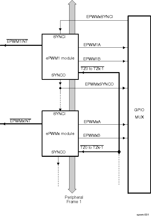 Figure 29-5 Multiple ePWM Modules
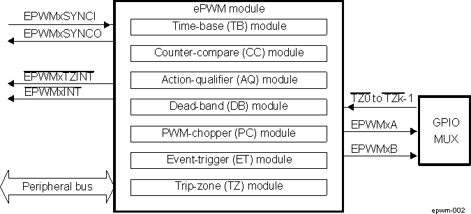 Figure 29-6 Submodules and Signal Connections for an ePWM Module
Figure 29-7 shows more internal details of a single ePWM module. The main signals used by the ePWM module are:
- PWM output signals (EPWMxA and EPWMxB). The PWM output signals are made available external to the device through the GPIO peripheral described in the system control and interrupts guide for your device.
- Trip-zone signals (
TZ0 to
TZk-1). These k input signals alert the ePWM module of an external fault condition. Each module on a device can be configured to either use or ignore any of the trip-zone signals. The trip-zone signal can be configured as an asynchronous input through the GPIO peripheral.
Note:
According to the device ePWMx (where x= 1to 3) trip zone i/f implementation, the number of input signals implemented is k=1, which means ONLY the ePWMx TZ0 input is available at chip level. Refer to the Section 29.1.3, for details on trip zone input implementation.
- Time-base synchronization input (EPWMxSYNCI) and output (EPWMxSYNCO) signals. The synchronization signals daisy chain the ePWM modules together. Each module can be configured to either use or ignore its synchronization input. The clock synchronization input and output signal are brought out to pins only for ePWM1 (ePWM module #1). The synchronization output for ePWM3 (EPWM3SYNCO) is also connected to the eCAP1SYNCI of the first enhanced capture module (eCAP1).
- Peripheral Bus. The peripheral bus is 32-bits wide and allows both 16-bit and 32-bit writes to the ePWM register file.
Figure 29-7 also shows the key internal submodule interconnect signals. Each submodule is described in Section 29.2.2.
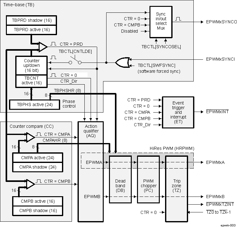 Figure 29-7 ePWM Submodules and Critical Internal Signal Interconnects
29.2.2 ePWM Functional Description
Seven submodules are included in each ePWM peripheral. There are some instances that include a high-resolution submodule that allows more precise control of the PWM outputs. Each of these submodules performs specific tasks that can be configured by software.
29.2.3 ePWM Submodule Features
Table 29-15 lists the eight key submodules together with a list of their main configuration parameters. For example, if you need to adjust or control the duty cycle of a PWM waveform, then you should see the counter-compare submodule in Section 29.2.14 for relevant details.
| Submodule | Configuration Parameter or Option | |
|---|---|---|
| Time-base (TB) |
| |
| Counter-compare (CC) |
| |
| Action-qualifier (AQ) |
| |
| Dead-band (DB) |
| |
| PWM-chopper (PC) |
| |
| Trip-zone (TZ) |
| |
Event-trigger (ET) |
| |
| High-Resolution PWM (HRPWM) |
| |
The system clock - SYSCLKOUT is the ePWM functional clock derived from the PWMSSn gateable interface and functional clock PWMSSn_GICLK, described in the Section 29.1.3.
Code examples are provided in the remainder of this chapter that show how to implement various ePWM module configurations. These examples use the constant definitions shown in Section 29.2.4.
29.2.4 Constant Definitions Used in the ePWM Code Examples
// TBCTL (Time-Base Control)
// = = = = = = = = = = = = = = = = = = = = = = = = = =
// TBCNT MODE bits
#define         TB_COUNT_UP        0x0
#define         TB_COUNT_DOWN      0x1
#define         TB_COUNT_UPDOWN    0x2
#define         TB_FREEZE          0x3
// PHSEN bit
#define         TB_DISABLE         0x0
#define         TB_ENABLE          0x1
// PRDLD bit
#define         TB_SHADOW          0x0
#define         TB_IMMEDIATE       0x1
// SYNCOSEL bits
#define         TB_SYNC_IN         0x0
#define         TB_CTR_ZERO        0x1
#define         TB_CTR_CMPB        0x2
#define         TB_SYNC_DISABLE    0x3
// HSPCLKDIV and CLKDIV bits
#define         TB_DIV1            0x0
#define         TB_DIV2            0x1
#define         TB_DIV4            0x2
// PHSDIR bit
#define         TB_DOWN            0x0
#define         TB_UP              0x1
// CMPCTL (Compare Control)
// = = = = = = = = = = = = = = = = = = = = = = = = = =
// LOADAMODE and LOADBMODE bits
#define CC_CTR_ZERO 0x0
#define CC_CTR_PRD 0x1
#define CC_CTR_ZERO_PRD 0x2
#define CC_LD_DISABLE 0x3
// SHDWAMODE and SHDWBMODE bits
#define CC_SHADOW 0x0
#define CC_IMMEDIATE 0x1
// AQCTLA and AQCTLB (Action-qualifier Control)
// = = = = = = = = = = = = = = = = = = = = = = = = = =
// ZRO, PRD, CAU, CAD, CBU, CBD bits
#define AQ_NO_ACTION 0x0
#define AQ_CLEAR 0x1
#define AQ_SET 0x2
#define AQ_TOGGLE 0x3
// DBCTL (Dead-Band Control)
// = = = = = = = = = = = = = = = = = = = = = = = = = =
// MODE bits
#define DB_DISABLE 0x0
#define DBA_ENABLE 0x1
#define DBB_ENABLE 0x2
#define DB_FULL_ENABLE 0x3
// POLSEL bits
#define DB_ACTV_HI 0x0
#define DB_ACTV_LOC 0x1
#define DB_ACTV_HIC 0x2
#define DB_ACTV_LO 0x3
// PCCTL (chopper control)
// = = = = = = = = = = = = = = = = = = = = = = = = = =
// CHPEN bit
#define CHP_ENABLE 0x0
#define CHP_DISABLE 0x1
// CHPFREQ bits
#define CHP_DIV1 0x0
#define CHP_DIV2 0x1
#define CHP_DIV3 0x2
#define CHP_DIV4 0x3
#define CHP_DIV5 0x4
#define CHP_DIV6 0x5
#define CHP_DIV7 0x6
#define CHP_DIV8 0x7
// CHPDUTY bits
#define CHP1_8TH 0x0
#define CHP2_8TH 0x1
#define CHP3_8TH 0x2
#define CHP4_8TH 0x3
#define CHP5_8TH 0x4
#define CHP6_8TH 0x5
#define CHP7_8TH 0x6
// TZSEL (Trip-zone Select)
// = = = = = = = = = = = = = = = = = = = = = = = = = =
// CBCn and OSHTn bits
#define TZ_ENABLE 0x0
#define TZ_DISABLE 0x1
// TZCTL (Trip-zone Control)
// = = = = = = = = = = = = = = = = = = = = = = = = = =
// TZA and TZB bits
#define TZ_HIZ 0x0
#define TZ_FORCE_HI 0x1
#define TZ_FORCE_LO 0x2
#define TZ_DISABLE 0x3
// ETSEL (Event-trigger Select)
// = = = = = = = = = = = = = = = = = = = = = = = = = =
// INTSEL, SOCASEL, SOCBSEL bits
#define ET_CTR_ZERO 0x1
#define ET_CTR_PRD 0x2
#define ET_CTRU_CMPA 0x4
#define ET_CTRD_CMPA 0x5
#define ET_CTRU_CMPB 0x6
#define ET_CTRD_CMPB 0x7
// ETPS (Event-trigger Prescale)
// = = = = = = = = = = = = = = = = = = = = = = = = = =
// INTPRD, SOCAPRD, SOCBPRD bits
#define ET_DISABLE 0x0
#define ET_1ST 0x1
#define ET_2ND 0x2
#define ET_3RD 0x329.2.5 Proper ePWM Interrupt Initialization Procedure
When the ePWM peripheral clock is enabled it may be possible that interrupt flags may be set due to spurious events due to the ePWM registers not being properly initialized. The proper procedure for initializing the ePWM peripheral is:
- Disable global interrupts (CPU INTM flag)
- Disable ePWM interrupts
- Initialize peripheral registers
- Clear any spurious ePWM flags
- Enable ePWM interrupts
- Enable global interrupts
29.2.6 ePWM Time-Base (TB) Submodule
Each ePWM module has its own time-base submodule that determines all of the event timing for the ePWM module. Built-in synchronization logic allows the time-base of multiple ePWM modules (ePWMx) to work together as a single system. Figure 29-8 illustrates the time-base module's place within the ePWM.
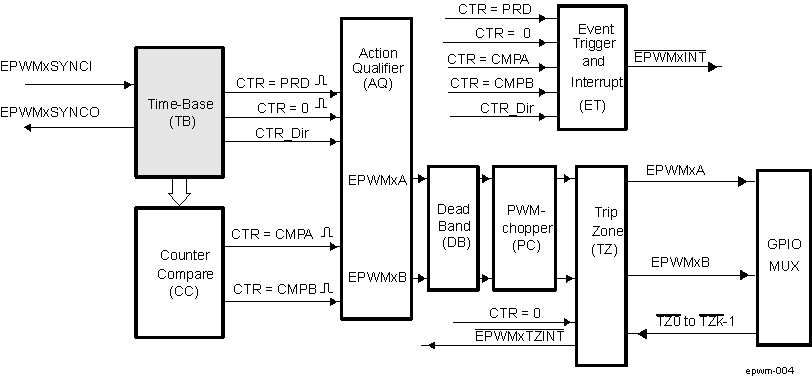 Figure 29-8 ePWM Time-Base Submodule Block Diagram
29.2.7 Purpose of the ePWM Time-Base Submodule
You can configure the time-base submodule for the following:
- Specify the ePWMx time-base counter (TBCNT) frequency or period in the EPWM_TBCNT register to control how often events occur.
- Manage time-base synchronization with other ePWMx modules.
- Maintain a phase relationship with other ePWMx modules.
- Set the time-base counter to count-up, count-down, or count-up-and-down mode.
- Generate the following events:
- TBCNT = PRD: Time-base counter (EPWM_TBCNT register) equal to the specified period in EPWM_TBPRD register (i.e. TBCNT = TBPRD) .
- TBCNT = 0: Time-base counter equal to zero (TBCNT = 0000h).
- Configure the rate of the time-base clock; a prescaled version of the CPU system clock (SYSCLKOUT). This allows the time-base counter to increment/decrement at a slower rate.
29.2.8 Controlling and Monitoring the ePWM Time-Base Submodule
Table 29-16 lists the registers used to control and monitor the time-base submodule.
| Acronym | Register Description | Address Offset | Shadowed |
|---|---|---|---|
| EPWM_TBCTL | Time-Base Control Register | 0h | No |
| EPWM_TBSTS | Time-Base Status Register | 2h | No |
| HRPWM_TBPHSHR | HRPWM extension Phase Register (1) | 4h | No |
| EPWM_TBPHS | Time-Base Phase Register | 6h | No |
| EPWM_TBCNT | Time-Base Counter Register | 8h | No |
| EPWM_TBPRD | Time-Base Period Register | Ah | Yes |
Figure 29-9 shows the critical signals and registers of the time-base submodule. Table 29-17 provides descriptions of the key signals associated with the time-base submodule.
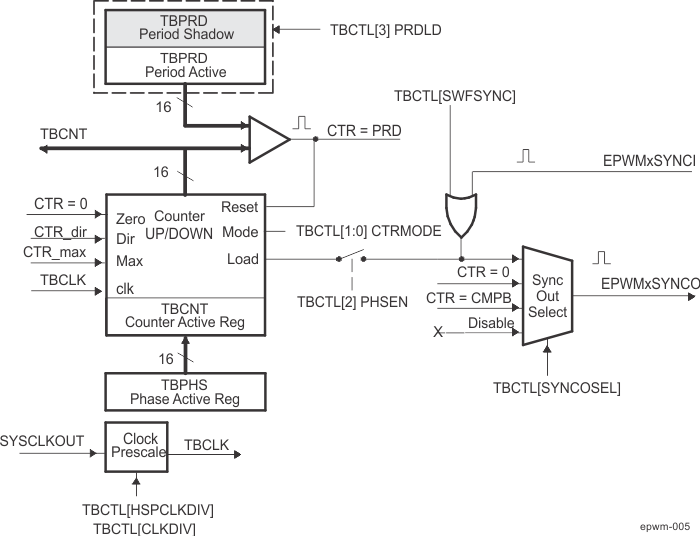 Figure 29-9 ePWM Time-Base Submodule Signals and Registers
| Signal | Description |
|---|---|
| EPWMxSYNCI | Time-base synchronization input. |
| Input pulse used to synchronize the time-base counter with the counter of ePWM module earlier in the synchronization chain. An ePWM peripheral can be configured to use or ignore this signal. For the first ePWM module (EPWM1) this signal comes from a device pin . For subsequent ePWM modules this signal is passed from another ePWM peripheral. For example, EPWM2SYNCI is generated by the ePWM1 peripheral and the EPWM3SYNCI is generated by ePWM2. See Section 29.2.11 for information on the synchronization order of a particular device. | |
| EPWMxSYNCO | Time-base synchronization output. |
This output pulse is used to synchronize the counter of an ePWM module later in the synchronization chain. The ePWM module generates this signal from one of three event sources:
| |
| TBCNT = PRD | Time-base counter equal to the specified period. |
| This signal is generated whenever the counter value is equal to the active period register value. That is when TBCNT = TBPRD. | |
| TBCNT = 0 | Time-base counter equal to zero. |
| This signal is generated whenever the counter value is zero. That is when TBCNT equals 0000h. | |
| TBCNT = CMPB | Time-base counter equal to active counter-compare B register (TBCNT = CMPB). |
| This event is generated by the counter-compare submodule and used by the synchronization out logic. | |
| CTR_dir | Time-base counter direction. |
| Indicates the current direction of the ePWM's time-base counter. This signal is high when the counter is increasing and low when it is decreasing. | |
| CTR_max | Time-base counter equal max value. (TBCNT = FFFFh) |
| Generated event when the EPWM_TBCNT value reaches its maximum value. This signal is only used only as a status bit. | |
| TBCLK | Time-base clock. |
| This is a prescaled version of the system clock - SYSCLKOUT(1) and is used by all submodules within the ePWMn. This clock determines the rate at which time-base counter increments or decrements. |
29.2.9 Calculating PWM Period and Frequency
The frequency of PWM events is controlled by the time-base period (EPWM_TBPRD) register and the mode of the time-base counter. Figure 29-10 shows the period (Tpwm) and frequency (Fpwm) relationships for the up-count, down-count, and up-down-count time-base counter modes when when the period is set to 4 (EPWM_TBPRD register bitfield TBPRD = 0x4). The time increment for each step is defined by the time-base clock (TBCLK) which is a prescaled version of the system clock (SYSCLKOUT).
The time-base counter has three modes of operation selected by the time-base control register (EPWM_TBCTL):
- Up-Down-Count Mode: In up-down-count mode, the time-base counter starts from zero and increments until the period (TBPRD) value is reached. When the period value is reached, the time-base counter then decrements until it reaches zero. At this point the counter repeats the pattern and begins to increment.
- Up-Count Mode: In this mode, the time-base counter starts from zero and increments until it reaches the value in the period register (TBPRD). When the period value is reached, the time-base counter resets to zero and begins to increment once again.
- Down-Count Mode: In down-count mode, the time-base counter starts from the period (TBPRD) value and decrements until it reaches zero. When it reaches zero, the time-base counter is reset to the period value and it begins to decrement once again.
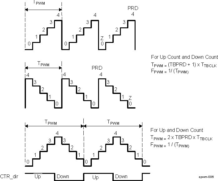 Figure 29-10 ePWM Time-Base Frequency and Period
29.2.10 ePWM Time-Base Period Shadow Register
The time-base period register (EPWM_TBPRD) has a shadow register. Shadowing allows the register update to be synchronized with the hardware. The following definitions are used to describe all shadow registers in the ePWM module:
- Active Register: The active register controls the hardware and is responsible for actions that the hardware causes or invokes.
- Shadow Register: The shadow register buffers or provides a temporary holding location for the active register. It has no direct effect on any control hardware. At a strategic point in time the shadow register's content is transferred to the active register. This prevents corruption or spurious operation due to the register being asynchronously modified by software.
The memory address of the shadow period register is the same as the active register. Which register is written to or read from is determined by the EPWM_TBCTL[3] PRDLD bit. This bit enables and disables the EPWM_TBPRD shadow register as follows:
- Time-Base Period Shadow Mode: The EPWM_TBPRD shadow register is enabled when EPWM_TBCTL[3] PRDLD = 0. Reads from and writes to the EPWM_TBPRD memory address go to the shadow register. The shadow register contents are transferred to the active register (EPWM_TBPRD (Active) ← EPWM_TBPRD (shadow)) when the time-base counter (register (EPWM_TBCNT) equals zero (TBCNT = 0000h). By default the EPWM_TBPRD shadow register is enabled.
- Time-Base Period Immediate Load Mode: If immediate load mode is selected (EPWM_TBCTL[3] PRDLD = 1), then a read from or a write to the TBPRD memory address goes directly to the active register.
29.2.11 ePWM Time-Base Counter Synchronization
A time-base synchronization scheme connects all of the ePWM modules on a device. Each ePWM module has a synchronization input (EPWMxSYNCI) and a synchronization output (EPWMxSYNCO). The input synchronization for the first instance (ePWM1) comes from an external pin . For the device ePWM environment sync pin details refer to the Section 29.1.2. The possible synchronization connections for the remaining ePWM modules is shown in Figure 29-11.
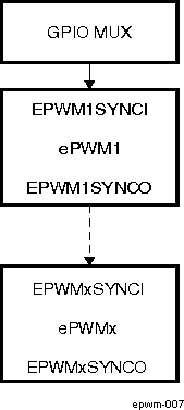 Figure 29-11 ePWM Time-Base Counter Synchronization Scheme 1
Each ePWM module can be configured to use or ignore the synchronization input. If the EPWM_TBCTL[2] PHSEN bit is set, then the time-base counter (TBCNT) of the ePWM module (register EPWM_TBCNT) will be automatically loaded with the phase register (EPWM_TBPHS) contents when one of the following conditions occur:
- EPWMxSYNCI: Synchronization Input Pulse: The value of the phase register is loaded into the counter register when an input synchronization pulse is detected (EPWM_TBPHS → EPWM_TBCNT). This operation occurs on the next valid time-base clock (TBCLK) edge.
- Software Forced Synchronization Pulse: Writing a 1 to the EPWM_TBCTL[6] SWFSYNC control bit invokes a software forced synchronization. This pulse is ORed with the synchronization input signal, and therefore has the same effect as a pulse on EPWMxSYNCI.
This feature enables the ePWM module to be automatically synchronized to the time base of another ePWM module. Lead or lag phase control can be added to the waveforms generated by different ePWM modules to synchronize them. In up-down-count mode, the EPWM_TBCTL[13] PHSDIR bit configures the direction of the time-base counter immediately after a synchronization event. The new direction is independent of the direction prior to the synchronization event. The TBPHS bit is ignored in count-up or count-down modes. See Figure 29-12 through Figure 29-15 for examples.
Clearing the EPWM_TBCTL[2] PHSEN bit configures the ePWM to ignore the synchronization input pulse. The synchronization pulse can still be allowed to flow-through to the EPWMxSYNCO and be used to synchronize other ePWM modules. In this way, you can set up a master time-base (for example, ePWM1) and downstream modules (ePWM2 - ePWMx) may elect to run in synchronization with the master.
29.2.12 Phase Locking the Time-Base Clocks of Multiple ePWM Modules
As already described in the Section 29.1.3.1.3, PWMSS1_TBCLKEN through PWMSS3_TBCLKEN bits in the CTRL_CORE_CONTROL_IO_2 register of the device Core Control Module can be used to individually control or globally synchronize the time-base clocks of all enabled ePWM modules on a device. When all PWMSSN_TBCLKEN (where n = 1 to 3) bits are set to 0b0, the time-base clocks of all ePWMx (where x = 1 to 3) modules are stopped (default). When all PWMSSn_TBCLKEN bits are simultaneously set in SW to 0b1, all ePWMx modules (x = 1 to 3) time-base clocks are started with the rising edge of TBCLK aligned. For perfectly synchronized TBCLKs, the prescaler bits in the EPWM_TBCTL register of each ePWM module must be set identically. The proper procedure for enabling the ePWM clocks is as follows:
- Enable the ePWM module clocks.
- Set PWMSSn_TBCLKEN = 0. This will stop the time-base clock within any enabled ePWMx module.
- Configure the prescaler values and desired ePWM modes per each involved ePWMx.
- Simultaneously set bits PWMSSn_TBCLKEN to 0b1 (where n = 1 to 3) 1.
29.2.13 ePWM Time-Base Counter Modes and Timing Waveforms
The time-base counter operates in one of four modes:
- Up-count mode which is asymmetrical.
- Down-count mode which is asymmetrical.
- Up-down-count which is symmetrical.
- Frozen where the time-base counter is held constant at the current value.
To illustrate the operation of the first three modes, Figure 29-12 to Figure 29-15 show when events are generated and how the time-base responds to an EPWMxSYNCI signal.
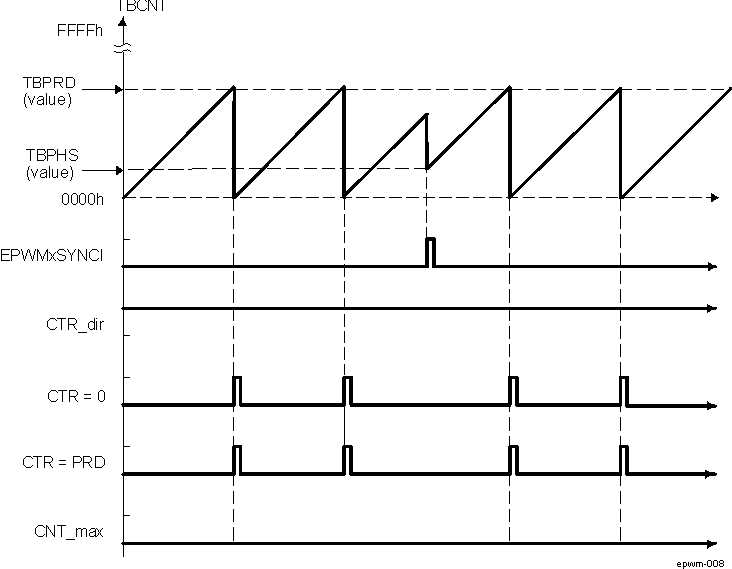 Figure 29-12 ePWM Time-Base Up-Count Mode Waveforms
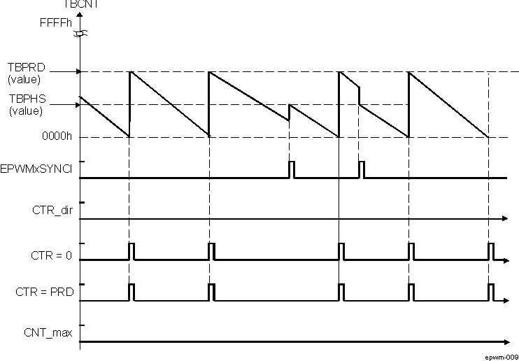 Figure 29-13 ePWM Time-Base Down-Count Mode Waveforms
![AM571x ePWM Time-Base Up-Down-Count Waveforms, EPWM_TBCTL[13] PHSDIR = 0 Count Down on Synchronization Event AM571x ePWM Time-Base Up-Down-Count Waveforms, EPWM_TBCTL[13] PHSDIR = 0 Count Down on Synchronization Event](/ods/images/SPRUHZ7K/GUID-A83A63B0-AA1B-4C21-A198-86B5A0594C52-low.gif) Figure 29-14 ePWM Time-Base Up-Down-Count Waveforms, EPWM_TBCTL[13] PHSDIR = 0 Count Down on
Figure 29-14 ePWM Time-Base Up-Down-Count Waveforms, EPWM_TBCTL[13] PHSDIR = 0 Count Down onSynchronization Event
![AM571x ePWM Time-Base Up-Down Count Waveforms, EPWM_TBCTL[13] PHSDIR = 1 Count Up on Synchronization Event AM571x ePWM Time-Base Up-Down Count Waveforms, EPWM_TBCTL[13] PHSDIR = 1 Count Up on Synchronization Event](/ods/images/SPRUHZ7K/GUID-2E54BBC3-BA08-4063-85AE-36FD319238F0-low.gif) Figure 29-15 ePWM Time-Base Up-Down Count Waveforms, EPWM_TBCTL[13] PHSDIR = 1 Count Up on
Figure 29-15 ePWM Time-Base Up-Down Count Waveforms, EPWM_TBCTL[13] PHSDIR = 1 Count Up onSynchronization Event
29.2.14 ePWM Counter-Compare (CC) Submodule
Figure 29-16 illustrates the counter-compare submodule within the ePWM. Figure 29-17 shows the basic structure of the counter-compare submodule.
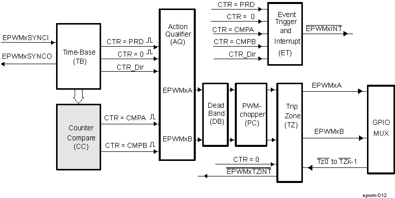 Figure 29-16 ePWM Counter-Compare Submodule
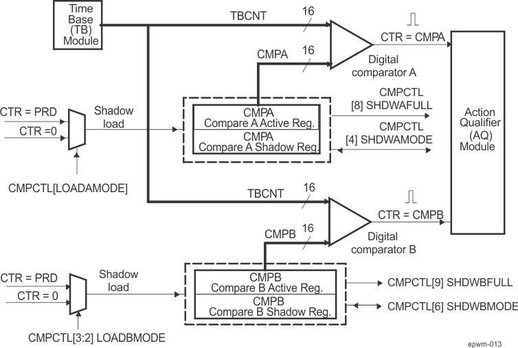 Figure 29-17 ePWM Counter-Compare Submodule Signals and Registers
29.2.15 Purpose of the ePWM Counter-Compare Submodule
The counter-compare submodule takes as input the time-base counter value. This value is continuously compared to the counter-compare A (EPWM_CMPA) and counter-compare B (EPWM_CMPB) registers. When the time-base counter is equal to one of the compare registers, the counter-compare unit generates an appropriate event.
The counter-compare submodule:
- Generates events based on programmable time stamps using the EPWM_CMPA and EPWM_CMPB registers
- TBCNT = CMPA: Time-base counter equals counter-compare A register (TBCNT = CMPA).
- TBCNT = CMPB: Time-base counter equals counter-compare B register (TBCNT = CMPB)
- Controls the PWM duty cycle if the action-qualifier submodule is configured appropriately
- Shadows new compare values to prevent corruption or glitches during the active PWM cycle
29.2.16 Controlling and Monitoring the ePWM Counter-Compare Submodule
Table 29-18 lists the registers used to control and monitor the counter-compare submodule. Table 29-19 lists the key signals associated with the counter-compare submodule.
| Acronym | Register Description | Address Offset | Shadowed |
|---|---|---|---|
| EPWM_CMPCTL | Counter-Compare Control Register. | Eh | No |
| HRPWM_CMPAHR | HRPWM Counter-Compare A Extension Register (1) | 10h | Yes |
| EPWM_CMPA | Counter-Compare A Register | 12h | Yes |
| EPWM_CMPB | Counter-Compare B Register | 14h | Yes |
| Signal | Description of Event | Register Bitfields Compared |
|---|---|---|
| TBCNT = CMPA | Time-base counter equal to the active counter-compare A value | TBCNT = CMPA |
| TBCNT = CMPB | Time-base counter equal to the active counter-compare B value | TBCNT = CMPB |
| TBCNT = PRD | Time-base counter equal to the active period. Used to load active counter-compare A and B registers from the shadow register | TBCNT = TBPRD |
| TBCNT = 0 | Time-base counter equal to zero. Used to load active counter-compare A and B registers from the shadow register | TBCNT = 0000h |
29.2.17 Operational Highlights for the ePWM Counter-Compare Submodule
The counter-compare submodule is responsible for generating two independent compare events based on two compare registers:
- TBCNT = CMPA: Time-base counter equal to counter-compare A register (EPWM_TBCNT = EPWM_CMPA).
- TBCNT = CMPB: Time-base counter equal to counter-compare B register (TBCNT = CMPB).
For up-count or down-count mode, each event occurs only once per cycle. For up-down-count mode each event occurs twice per cycle, if the compare value is between 0000h and TBPRD; and occurs once per cycle, if the compare value is equal to 0000h or equal to TBPRD. These events are fed into the action-qualifier submodule where they are qualified by the counter direction and converted into actions if enabled. Refer to Section 29.2.20 for more details.
The counter-compare registers EPWM_CMPA and EPWM_CMPB each have an associated shadow register. Shadowing provides a way to keep updates to the registers synchronized with the hardware. When shadowing is used, updates to the active registers only occurs at strategic points. This prevents corruption or spurious operation due to the register being asynchronously modified by software. The memory address of the active register and the shadow register is identical. Which register is written to or read from is determined by the EPWM_CMPCTL[4] SHDWAMODE and EPWM_CMPCTL[6] SHDWBMODE bits. These bits enable and disable the EPWM_CMPA shadow register and EPWM_CMPB shadow register respectively. The behavior of the two load modes is described below:
- Shadow Mode: The shadow mode for the EPWM_CMPA is enabled by clearing the EPWM_CMPCTL[4] SHDWAMODE bit and the shadow register for CMPB is enabled by clearing the EPWM_CMPCTL[6] SHDWBMODE bit. Shadow mode is enabled by default for both EPWM_CMPA and EPWM_CMPB.
If the shadow register is enabled then the content of the shadow register is transferred to the active register on one of the following events:
- TBCNT = PRD: Time-base counter equal to the period (TBCNT = TBPRD).
- TBCNT = 0: Time-base counter equal to zero (TBCNT = 0000h)
- Both TBCNT = PRD and TBCNT = 0
Which of these three events is specified by the EPWM_CMPCTL[1:0] LOADAMODE and EPWM_CMPCTL[3:2] LOADBMODE register bits. Only the active register contents are used by the counter-compare submodule to generate events to be sent to the action-qualifier.
- Immediate Load Mode: If immediate load mode is selected (EPWM_TBCTL[4] SHDWAMODE = 1 or EPWM_TBCTL[6] SHDWBMODE = 1), then a read from or a write to the register will go directly to the active register.
29.2.18 ePWM Count Mode Timing Waveforms
The counter-compare module can generate compare events in all three count modes:
- Up-count mode: used to generate an asymmetrical PWM waveform.
- Down-count mode: used to generate an asymmetrical PWM waveform.
- Up-down-count mode: used to generate a symmetrical PWM waveform.
To best illustrate the operation of the first three modes, the timing diagrams in Figure 29-18 to Figure 29-21 show when events are generated and how the EPWMxSYNCI signal interacts.
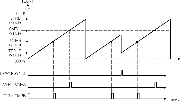
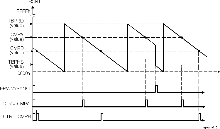 Figure 29-19 ePWM Counter-Compare Events in Down-Count Mode
![AM571x ePWM Counter-Compare Events in Up-Down-Count Mode, EPWM_TBCTL[13] PHSDIR = 0 Count Down on Synchronization Event AM571x ePWM Counter-Compare Events in Up-Down-Count Mode, EPWM_TBCTL[13] PHSDIR = 0 Count Down on Synchronization Event](/ods/images/SPRUHZ7K/GUID-45B68F11-0221-4B52-8DAB-050C4F7BC402-low.gif) Figure 29-20 ePWM Counter-Compare Events in Up-Down-Count Mode, EPWM_TBCTL[13] PHSDIR = 0 Count Down on Synchronization Event
Figure 29-20 ePWM Counter-Compare Events in Up-Down-Count Mode, EPWM_TBCTL[13] PHSDIR = 0 Count Down on Synchronization Event![AM571x ePWM Counter-Compare Events in Up-Down-Count Mode, EPWM_TBCTL[13] PHSDIR = 1 Count Up on Synchronization Event AM571x ePWM Counter-Compare Events in Up-Down-Count Mode, EPWM_TBCTL[13] PHSDIR = 1 Count Up on Synchronization Event](/ods/images/SPRUHZ7K/GUID-09F59A44-F49B-462B-A944-D97BA9379D5A-low.gif) Figure 29-21 ePWM Counter-Compare Events in Up-Down-Count Mode, EPWM_TBCTL[13] PHSDIR = 1 Count Up on Synchronization Event
Figure 29-21 ePWM Counter-Compare Events in Up-Down-Count Mode, EPWM_TBCTL[13] PHSDIR = 1 Count Up on Synchronization Event29.2.19 ePWM Action-Qualifier (AQ) Submodule
Figure 29-22 shows the action-qualifier (AQ) submodule (see shaded block) in the ePWM system. The action-qualifier submodule has the most important role in waveform construction and PWM generation. It decides which events are converted into various action types, thereby producing the required switched waveforms at the EPWMxA and EPWMxB outputs.
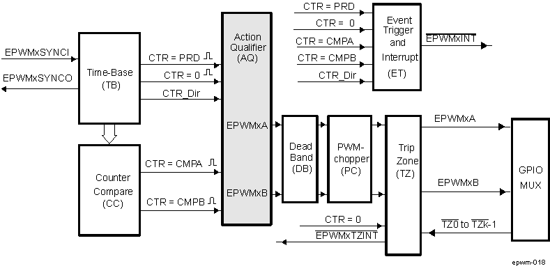 Figure 29-22 ePWM Action-Qualifier Submodule
29.2.20 Purpose of the ePWM Action-Qualifier Submodule
The action-qualifier submodule is responsible for the following:
- Qualifying and generating actions (set, clear, toggle) based on the following events:
- TBCNT = PRD: Time-base counter equal to the period (TBCNT = TBPRD)
- TBCNT = 0: Time-base counter equal to zero (TBCNT = 0000h)
- TBCNT = CMPA: Time-base counter equal to the counter-compare A register (TBCNT = CMPA)
- TBCNT = CMPB: Time-base counter equal to the counter-compare B register (TBCNT = CMPB)
- Managing priority when these events occur concurrently
- Providing independent control of events when the time-base counter is increasing and when it is decreasing.
29.2.21 Controlling and Monitoring the ePWM Action-Qualifier Submodule
Table 29-20 lists the registers used to control and monitor the action-qualifier submodule.
| Acronym | Register Description | Address Offset | Shadowed |
|---|---|---|---|
| EPWM_AQCTLA | Action-Qualifier Control Register For Output A (EPWMxA) | 16h | No |
| EPWM_AQCTLB | Action-Qualifier Control Register For Output B (EPWMxB) | 18h | No |
| EPWM_AQSFRC | Action-Qualifier Software Force Register | 1Ah | No |
| EPWM_AQCSFRC | Action-Qualifier Continuous Software Force | 1Ch | Yes |
The action-qualifier submodule is based on event-driven logic. It can be thought of as a programmable cross switch with events at the input and actions at the output, all of which are software controlled via the set of registers shown in Figure 29-23. The possible input events are summarized again in Table 29-21.
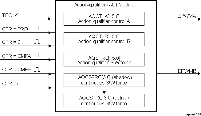 Figure 29-23 ePWM Action-Qualifier Submodule Inputs and Outputs
| Signal | Description | Register Bitfield Compared |
|---|---|---|
| TBCNT = PRD | Time-base counter equal to the period value | TBCNT = TBPRD |
| TBCNT = 0 | Time-base counter equal to zero | TBCNT = 0000h |
| TBCNT = CMPA | Time-base counter equal to the counter-compare A | TBCNT = CMPA |
| TBCNT = CMPB | Time-base counter equal to the counter-compare B | TBCNT = CMPB |
| Software forced event | Asynchronous event initiated by software |
The software forced action is a useful asynchronous event. This control is handled by registers EPWM_AQSFRC and EPWM_AQCSFRC.
The action-qualifier submodule controls how the two outputs EPWMxA and EPWMxB behave when a particular event occurs. The event inputs to the action-qualifier submodule are further qualified by the counter direction (up or down). This allows for independent action on outputs on both the count-up and count-down phases.
The possible actions imposed on outputs EPWMxA and EPWMxB are:
- Set High: Set output EPWMxA or EPWMxB to a high level.
- Clear Low: Set output EPWMxA or EPWMxB to a low level.
- Toggle: If EPWMxA or EPWMxB is currently pulled high, then pull the output low. If EPWMxA or EPWMxB is currently pulled low, then pull the output high.
- Do Nothing: Keep outputs EPWMxA and EPWMxB at same level as currently set. Although the "Do Nothing" option prevents an event from causing an action on the EPWMxA and EPWMxB outputs, this event can still trigger interrupts. See the event-trigger submodule description in Section 29.2.41 for details.
Actions are specified independently for either output (EPWMxA or EPWMxB). Any or all events can be configured to generate actions on a given output. For example, both TBCNT = CMPA and TBCNT = CMPB can operate on output EPWMxA. All qualifier actions are configured via the control registers found at the end of this section.
For clarity, the drawings in this chapter use a set of symbolic actions. These symbols are summarized in Figure 29-24. Each symbol represents an action as a marker in time. Some actions are fixed in time (zero and period) while the CMPA and CMPB actions are moveable and their time positions are programmed via the counter-compare A and B registers, respectively. To turn off or disable an action, use the "Do Nothing option"; it is the default at reset.
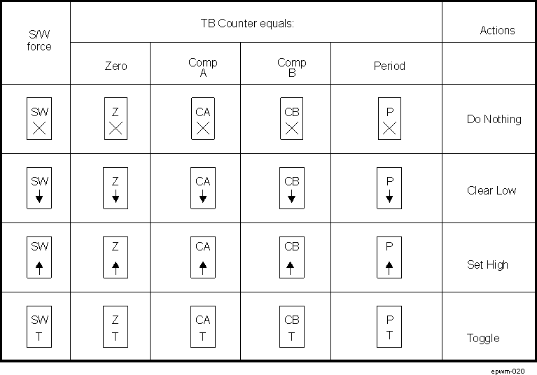 Figure 29-24 Possible Action-Qualifier Actions for EPWMxA and EPWMxB Outputs
29.2.22 ePWM Action-Qualifier Event Priority
It is possible for the ePWM action qualifier to receive more than one event at the same time. In this case events are assigned a priority by the hardware. The general rule is events occurring later in time have a higher priority and software forced events always have the highest priority. The event priority levels for up-down-count mode are shown in Table 29-22. A priority level of 1 is the highest priority and level 7 is the lowest. The priority changes slightly depending on the direction of TBCNT.
| Priority Level | Event if TBCNT is Incrementing TBCNT = 0 up to TBCNT = TBPRD | Event if TBCNT is Decrementing TBCNT = TBPRD down to TBCNT = 1 |
|---|---|---|
| 1 (Highest) | Software forced event | Software forced event |
| 2 | Counter equals CMPB on up-count (CBU) | Counter equals CMPB on down-count (CBD) |
| 3 | Counter equals CMPA on up-count (CAU) | Counter equals CMPA on down-count (CAD) |
| 4 | Counter equals zero | Counter equals period (TBPRD in EPWM_TBPRD active register) |
| 5 | Counter equals CMPB on down-count (CBD) (1) | Counter equals CMPB on up-count (CBU) (1) |
| 6 (Lowest) | Counter equals CMPA on down-count (CAD) (1) | Counter equals CMPA on up-count (CBU) (1) |
Table 29-23 shows the action-qualifier priority for up-count mode. In this case, the counter direction is always defined as up and thus down-count events will never be taken.
| Priority Level | Event |
|---|---|
| 1 (Highest) | Software forced event |
| 2 | Counter equal to period (TBPRD) |
| 3 | Counter equal to CMPB on up-count (CBU) |
| 4 | Counter equal to CMPA on up-count (CAU) |
| 5 (Lowest) | Counter equal to Zero |
Table 29-24 shows the action-qualifier priority for down-count mode. In this case, the counter direction is always defined as down and thus up-count events will never be taken.
| Priority Level | Event |
|---|---|
| 1 (Highest) | Software forced event |
| 2 | Counter equal to Zero |
| 3 | Counter equal to CMPB on down-count (CBD) |
| 4 | Counter equal to CMPA on down-count (CAD) |
| 5 (Lowest) | Counter equal to period (TBPRD) |
It is possible to set the compare value greater than the period. In this case the action will take place as shown in Table 29-25.
| Counter Mode | Compare on Up-Count Event CAU/CBU | Compare on Down-Count Event CAU/CBU |
|---|---|---|
| Up-Count Mode | If CMPA/CMPB ≤ TBPRD period, then the event occurs on a compare match (TBCNT = CMPA or CMPB). | Never occurs. |
| If CMPA/CMPB > TBPRD, then the event will not occur. | ||
| Down-Count Mode | Never occurs. | If CMPA/CMPB < TBPRD, the event will occur on a compare match (TBCNT = CMPA or CMPB). |
| If CMPA/CMPB ≥ TBPRD, the event will occur on a period match (TBCNT = TBPRD). | ||
| Up-Down-Count Mode | If CMPA/CMPB < TBPRD and the counter is incrementing, the event occurs on a compare match (TBCNT = CMPA or CMPB). | If CMPA/CMPB < TBPRD and the counter is decrementing, the event occurs on a compare match (TBCNT = CMPA or CMPB). |
| If CMPA/CMPB is ≥ TBPRD, the event will occur on a period match (TBCNT = TBPRD). | If CMPA/CMPB ≥ TBPRD, the event occurs on a period match (TBCNT = TBPRD). |
29.2.23 Waveforms for Common ePWM Configurations
The waveforms in this chapter show the ePWMs behavior for a static compare register value. In a running system, the active compare registers (EPWM_CMPA and EPWM_CMPB) are typically updated from their respective shadow registers once every period. The user specifies when the update will take place; either when the time-base counter reaches zero or when the time-base counter reaches period. There are some cases when the action based on the new value can be delayed by one period or the action based on the old value can take effect for an extra period. Some PWM configurations avoid this situation. These include, but are not limited to, the following:
Use up-down-count mode to generate a symmetric PWM:
- If you load EPWM_CMPA/EPWM_CMPB on zero, then use EPWM_CMPA/EPWM_CMPB values greater than or equal to 1.
- If you load EPWM_CMPA/EPWM_CMPB on period, then use EPWM_CMPA/EPWM_CMPB values less than or equal to TBPRD - 1.
This means there will always be a pulse of at least one TBCLK cycle in a PWM period which, when very short, tend to be ignored by the system.
Use up-down-count mode to generate an asymmetric PWM:
- To achieve 50%-0% asymmetric PWM use the following configuration: Load EPWM_CMPA/EPWM_CMPB on period and use the period action to clear the PWM and a compare-up action to set the PWM. Modulate the compare value from 0 to TBPRD to achieve 50%-0% PWM duty.
When using up-count mode to generate an asymmetric PWM:
Figure 29-25 shows how a symmetric PWM waveform can be generated using the up-down-count mode of the TBCNT. In this mode 0%-100% DC modulation is achieved by using equal compare matches on the up count and down count portions of the waveform. In the example shown, CMPA is used to make the comparison. When the counter is incrementing the CMPA match will pull the PWM output high. Likewise, when the counter is decrementing the compare match will pull the PWM signal low. When CMPA = 0, the PWM signal is low for the entire period giving the 0% duty waveform. When EPWM_CMPA = EPWM_TBPRD, the PWM signal is high achieving 100% duty.
When using this configuration in practice, if you load CMPA/CMPB on zero, then use CMPA/CMPB values greater than or equal to 1. If you load CMPA/CMPB on period, then use CMPA/CMPB values less than or equal to TBPRD-1. This means there will always be a pulse of at least one TBCLK cycle in a PWM period which, when very short, tend to be ignored by the system.
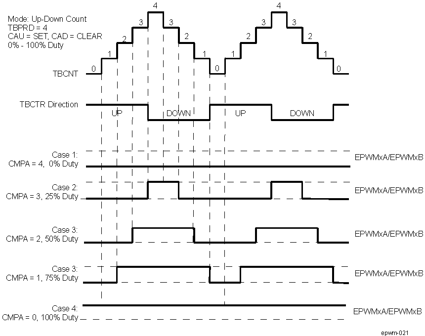 Figure 29-25 ePWM Up-Down-Count Mode Symmetrical Waveform
The PWM waveforms in Figure 29-26 through Figure 29-31 show some common action-qualifier configurations. Some conventions used in the figures are as follows:
- TBPRD, CMPA, and CMPB refer to the value written in their respective registers (EPWM_TBPRD, EPWM_CMPA, and EPWM_CMPB). The active register, not the shadow register, is used by the hardware.
- CMPx, refers to either CMPA or CMPB.
- EPWMxA and EPWMxB refer to the output signals from ePWMx
- Up-Down means Count-up-and-down mode, Up means up-count mode and Dwn means down-count mode
- Sym = Symmetric, Asym = Asymmetric
Table 29-26 and Table 29-27 contains initialization and runtime register configurations for the waveforms in Figure 29-26.
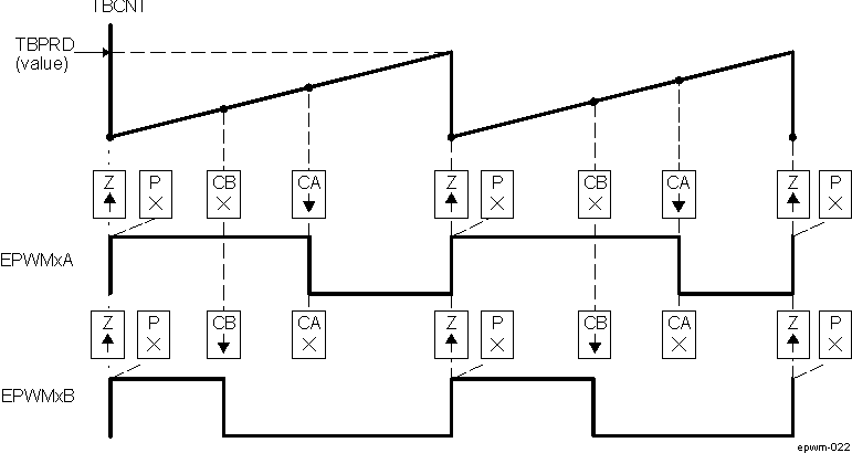
| Register | Bitfield | Value | Comments |
|---|---|---|---|
| EPWM_TBPRD | TBPRD | 600 (258h) | Period = 601 TBCLK counts |
| EPWM_TBPHS | TBPHS | 0 | Clear Phase Register to 0 |
| EPWM_TBCNT | TBCNT | 0 | Clear TB counter |
| EPWM_TBCTL | CTRMODE | TB_UP | |
| PHSEN | TB_DISABLE | Phase loading disabled | |
| PRDLD | TB_SHADOW | ||
| SYNCOSEL | TB_SYNC_DISABLE | ||
| HSPCLKDIV | TB_DIV1 | TBCLK = SYSCLKOUT | |
| CLKDIV | TB_DIV1 | ||
| EPWM_CMPA | CMPA | 350 (15Eh) | Compare A = 350 TBCLK counts |
| EPWM_CMPB | CMPB | 200 (C8h) | Compare B = 200 TBCLK counts |
| EPWM_CMPCTL | SHDWAMODE | CC_SHADOW | |
| SHDWBMODE | CC_SHADOW | ||
| LOADAMODE | CC_CTR_ZERO | Load on TBCNT = 0 | |
| LOADBMODE | CC_CTR_ZERO | Load on TBCNT = 0 | |
| EPWM_AQCTLA | ZRO | AQ_SET | |
| CAU | AQ_CLEAR | ||
| EPWM_AQCTLB | ZRO | AQ_SET | |
| CBU | AQ_CLEAR |
| Register | Bitfield | Value | Comments |
|---|---|---|---|
| EPWM_CMPA | CMPA | Duty1A | Adjust duty for output EPWM1A |
| EPWM_CMPB | CMPB | Duty1B | Adjust duty for output EPWM1B |
Table 29-28 and Table 29-29 contains initialization and runtime register configurations for the waveforms in Figure 29-27.
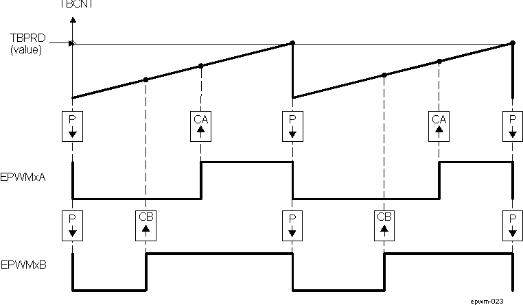
| Register | Bitfiled | Value | Comments |
|---|---|---|---|
| EPWM_TBPRD | TBPRD | 600 (258h) | Period = 601 TBCLK counts |
| EPWM_TBPHS | TBPHS | 0 | Clear Phase Register to 0 |
| EPWM_TBCNT | TBCNT | 0 | Clear TB counter |
| EPWM_TBCTL | CTRMODE | TB_UP | |
| PHSEN | TB_DISABLE | Phase loading disabled | |
| PRDLD | TB_SHADOW | ||
| SYNCOSEL | TB_SYNC_DISABLE | ||
| HSPCLKDIV | TB_DIV1 | TBCLK = SYSCLKOUT | |
| CLKDIV | TB_DIV1 | ||
| EPWM_CMPA | CMPA | 350 (15Eh) | Compare A = 350 TBCLK counts |
| EPWM_CMPB | CMPB | 200 (C8h) | Compare B = 200 TBCLK counts |
| EPWM_CMPCTL | SHDWAMODE | CC_SHADOW | |
| SHDWBMODE | CC_SHADOW | ||
| LOADAMODE | CC_CTR_ZERO | Load on TBCNT = 0 | |
| LOADBMODE | CC_CTR_ZERO | Load on TBCNT = 0 | |
| EPWM_AQCTLA | PRD | AQ_CLEAR | |
| CAU | AQ_SET | ||
| EPWM_AQCTLB | PRD | AQ_CLEAR | |
| CBU | AQ_SET |
| Register | Bit | Value | Comments |
|---|---|---|---|
| EPWM_CMPA | CMPA | Duty1A | Adjust duty for output EPWM1A |
| EPWM_CMPB | CMPB | Duty1B | Adjust duty for output EPWM1B |
Table 29-30 and Table 29-31 contains initialization and runtime register configurations for the waveforms Figure 29-28. Use the code in Section 29.2.4 to define the headers.
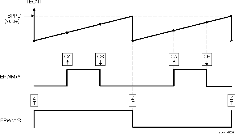
| Register | Bitfield | Value | Comments |
|---|---|---|---|
| EPWM_TBPRD | TBPRD | 600 (258h) | Period = 601 TBCLK counts |
| EPWM_TBPHS | TBPHS | 0 | Clear Phase Register to 0 |
| EPWM_TBCNT | TBCNT | 0 | Clear TB counter |
| EPWM_TBCTL | CTRMODE | TB_UP | |
| PHSEN | TB_DISABLE | Phase loading disabled | |
| PRDLD | TB_SHADOW | ||
| SYNCOSEL | TB_SYNC_DISABLE | ||
| HSPCLKDIV | TB_DIV1 | TBCLK = SYSCLKOUT | |
| CLKDIV | TB_DIV1 | ||
| EPWM_CMPA | CMPA | 200 (C8h) | Compare A = 200 TBCLK counts |
| EPWM_CMPB | CMPB | 400 (190h) | Compare B = 400 TBCLK counts |
| EPWM_CMPCTL | SHDWAMODE | CC_SHADOW | |
| SHDWBMODE | CC_SHADOW | ||
| LOADAMODE | CC_CTR_ZERO | Load on TBCNT = 0 | |
| LOADBMODE | CC_CTR_ZERO | Load on TBCNT = 0 | |
| EPWM_AQCTLA | CAU | AQ_SET | |
| CBU | AQ_CLEAR | ||
| EPWM_AQCTLB | ZRO | AQ_TOGGLE |
| Register | Bitfield | Value | Comments |
|---|---|---|---|
| EPWM_CMPA | CMPA | EdgePosA | Adjust duty for output EPWM1A |
| EPWM_CMPB | CMPB | EdgePosB |
Table 29-32 and Table 29-33 contains initialization and runtime register configurations for the waveforms in Figure 29-29. Use the code in Section 29.2.4 to define the headers.
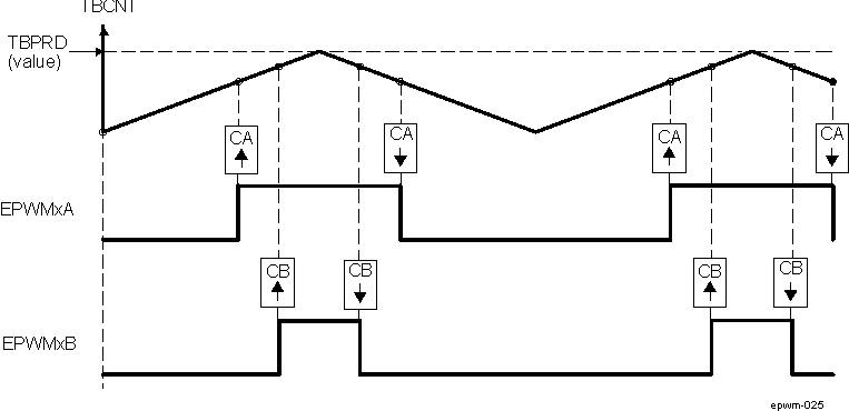
| Register | Bitfield | Value | Comments |
|---|---|---|---|
| EPWM_TBPRD | TBPRD | 600 (258h) | Period = 601 TBCLK counts |
| EPWM_TBPHS | TBPHS | 0 | Clear Phase Register to 0 |
| EPWM_TBCNT | TBCNT | 0 | Clear TB counter |
| EPWM_TBCTL | CTRMODE | TB_UPDOWN | |
| PHSEN | TB_DISABLE | Phase loading disabled | |
| PRDLD | TB_SHADOW | ||
| SYNCOSEL | TB_SYNC_DISABLE | ||
| HSPCLKDIV | TB_DIV1 | TBCLK = SYSCLKOUT | |
| CLKDIV | TB_DIV1 | ||
| EPWM_CMPA | CMPA | 400 (190h) | Compare A = 400 TBCLK counts |
| EPWM_CMPB | CMPB | 500 (1F4h) | Compare B = 500 TBCLK counts |
| EPWM_CMPCTL | SHDWAMODE | CC_SHADOW | |
| SHDWBMODE | CC_SHADOW | ||
| LOADAMODE | CC_CTR_ZERO | Load on TBCNT = 0 | |
| LOADBMODE | CC_CTR_ZERO | Load on TBCNT = 0 | |
| EPWM_AQCTLA | CAU | AQ_SET | |
| CAD | AQ_CLEAR | ||
| EPWM_AQCTLB | CBU | AQ_SET | |
| CBD | AQ_CLEAR |
| Register | Bitfield | Value | Comments |
|---|---|---|---|
| EPWM_CMPA | CMPA | Duty1A | Adjust duty for output EPWM1A |
| EPWM_CMPB | CMPB | Duty1B | Adjust duty for output EPWM1B |
Table 29-34 and Table 29-35 contains initialization and runtime register configurations for the waveforms in Figure 29-30. Use the code in Section 29.2.4 to define the headers.
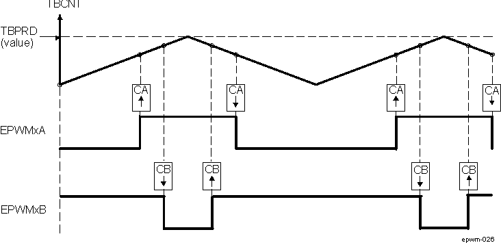
| Register | Bitfield | Value | Comments |
|---|---|---|---|
| EPWM_TBPRD | TBPRD | 600 (258h) | Period = 601 TBCLK counts |
| EPWM_TBPHS | TBPHS | 0 | Clear Phase Register to 0 |
| EPWM_TBCNT | TBCNT | 0 | Clear TB counter |
| EPWM_TBCTL | CTRMODE | TB_UPDOWN | |
| PHSEN | TB_DISABLE | Phase loading disabled | |
| PRDLD | TB_SHADOW | ||
| SYNCOSEL | TB_SYNC_DISABLE | ||
| HSPCLKDIV | TB_DIV1 | TBCLK = SYSCLKOUT | |
| CLKDIV | TB_DIV1 | ||
| EPWM_CMPA | CMPA | 350 (15Eh) | Compare A = 350 TBCLK counts |
| EPWM_CMPB | CMPB | 400 (190h) | Compare B = 400 TBCLK counts |
| EPWM_CMPCTL | SHDWAMODE | CC_SHADOW | |
| SHDWBMODE | CC_SHADOW | ||
| LOADAMODE | CC_CTR_ZERO | Load on TBCNT = 0 | |
| LOADBMODE | CC_CTR_ZERO | Load on TBCNT = 0 | |
| EPWM_AQCTLA | CAU | AQ_SET | |
| CAD | AQ_CLEAR | ||
| EPWM_AQCTLB | CBU | AQ_CLEAR | |
| CBD | AQ_SET |
| Register | Bitfield | Value | Comments |
|---|---|---|---|
| EPWM_CMPA | CMPA | Duty1A | Adjust duty for output EPWM1A |
| EPWM_CMPB | CMPB | Duty1B | Adjust duty for output EPWM1B |
Table 29-36 and Table 29-37 contains initialization and runtime register configurations for the waveforms in Figure 29-31. Use the code in Section 29.2.4 to define the headers.
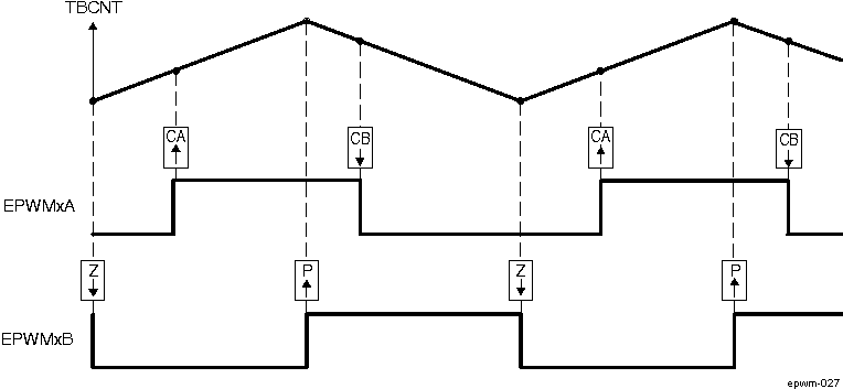
| Register | Bitfield | Value | Comments |
|---|---|---|---|
| EPWM_TBPRD | TBPRD | 600 (258h) | Period = 601 TBCLK counts |
| EPWM_TBPHS | TBPHS | 0 | Clear Phase Register to 0 |
| EPWM_TBCNT | TBCNT | 0 | Clear TB counter |
| EPWM_TBCTL | CTRMODE | TB_UPDOWN | |
| PHSEN | TB_DISABLE | Phase loading disabled | |
| PRDLD | TB_SHADOW | ||
| SYNCOSEL | TB_SYNC_DISABLE | ||
| HSPCLKDIV | TB_DIV1 | TBCLK = SYSCLKOUT | |
| CLKDIV | TB_DIV1 | ||
| EPWM_CMPA | CMPA | 250 (FAh) | Compare A = 250 TBCLK counts |
| EPWM_CMPB | CMPB | 450 (1C2h) | Compare B = 450 TBCLK counts |
| EPWM_CMPCTL | SHDWAMODE | CC_SHADOW | |
| SHDWBMODE | CC_SHADOW | ||
| LOADAMODE | CC_CTR_ZERO | Load on TBCNT = 0 | |
| LOADBMODE | CC_CTR_ZERO | Load on TBCNT = 0 | |
| EPWM_AQCTLA | CAU | AQ_SET | |
| CBD | AQ_CLEAR | ||
| EPWM_AQCTLB | ZRO | AQ_CLEAR | |
| PRD | AQ_SET |
| Register | Bitfield | Value | Comments |
|---|---|---|---|
| EPWM_CMPA | CMPA | EdgePosA | Adjust duty for output EPWM1A |
| EPWM_CMPB | CMPB | EdgePosB |
29.2.24 ePWM Dead-Band Generator (DB) Submodule
Figure 29-32 illustrates the dead-band generator submodule within the ePWM module.
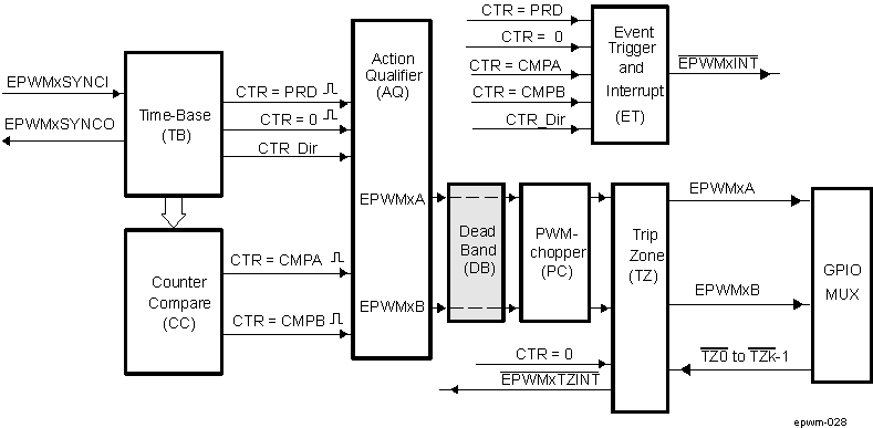 Figure 29-32 Dead-Band Generator Submodule
29.2.25 Purpose of the ePWM Dead-Band Submodule
The "Action-qualifier (AQ) Module" section discussed how it is possible to generate the required dead-band by having full control over edge placement using both the CMPA and CMPB resources of the ePWM module. However, if the more classical edge delay-based dead-band with polarity control is required, then the dead-band generator submodule should be used.
The key functions of the dead-band generator submodule are:
- Generating appropriate signal pairs (EPWMxA and EPWMxB) with dead-band relationship from a single EPWMxA input
- Programming signal pairs for:
- Active high (AH)
- Active low (AL)
- Active high complementary (AHC)
- Active low complementary (ALC)
- Adding programmable delay to rising edges (RED)
- Adding programmable delay to falling edges (FED)
- Can be totally bypassed from the signal path (note dotted lines in diagram)
29.2.26 Controlling and Monitoring the ePWM Dead-Band Submodule
The dead-band generator submodule operation is controlled and monitored via the following registers:
| Acronym | Register Description | Address Offset | Shadowed |
|---|---|---|---|
| EPWM_DBCTL | Dead-Band Control Register | 1Eh | No |
| EPWM_DBRED | Dead-Band Rising Edge Delay Count Register | 20h | No |
| EPWM_DBFED | Dead-Band Falling Edge Delay Count Register | 22h | No |
29.2.27 Operational Highlights for the ePWM Dead-Band Generator Submodule
The following sections provide the operational highlights.
The dead-band submodule has two groups of independent selection options as shown in Figure 29-33.
- Input Source Selection: The input signals to the dead-band module are the EPWMxA and EPWMxB output signals from the action-qualifier. In this section they will be referred to as EPWMxA In and EPWMxB In. Using the EPWM_DBCTL[5:4] IN_MODE control bits, the signal source for each delay, falling-edge or rising-edge, can be selected:
- EPWMxA In is the source for both falling-edge and rising-edge delay. This is the default mode.
- EPWMxA In is the source for falling-edge delay, EPWMxB In is the source for rising-edge delay.
- EPWMxA In is the source for rising edge delay, EPWMxB In is the source for falling-edge delay.
- EPWMxB In is the source for both falling-edge and rising-edge delay.
- Output Mode Control: The output mode is configured by way of the EPWM_DBCTL[1:0] OUT_MODE bits. These bits determine if the falling-edge delay, rising-edge delay, neither, or both are applied to the input signals.
- Polarity Control: The polarity control (EPWM_DBCTL[3:2] POLSEL) allows you to specify whether the rising-edge delayed signal and/or the falling-edge delayed signal is to be inverted before being sent out of the dead-band submodule.
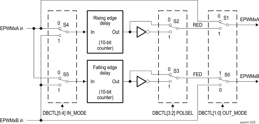 Figure 29-33 Configuration Options for the ePWM Dead-Band Generator Submodule
Although all combinations are supported, not all are typical usage modes. Table 29-39 lists some classical dead-band configurations. These modes assume that the EPWM_DBCTL[5:4] IN_MODE is configured such that EPWMxA In is the source for both falling-edge and rising-edge delay. Enhanced, or non-traditional modes can be achieved by changing the input signal source. The modes shown in Table 29-39 fall into the following categories:
- Mode 1: Bypass both falling-edge delay (FED) and rising-edge delay (RED) Allows you to fully disable the dead-band submodule from the PWM signal path.
- Mode 2-5: Classical Dead-Band Polarity Settings These represent typical polarity configurations that should address all the active high/low modes required by available industry power switch gate drivers. The waveforms for these typical cases are shown in Figure 29-34. Note that to generate equivalent waveforms to Figure 29-34, configure the action-qualifier submodule to generate the signal as shown for EPWMxA.
- Mode 6: Bypass rising-edge-delay and Mode 7: Bypass falling-edge-delay Finally the last two entries in Table 29-39 show combinations where either the falling-edge-delay (FED) or rising-edge-delay (RED) blocks are bypassed.
| Mode | Mode Description (1) | EPWM_DBCTL[3:2] POLSEL | EPWM_DBCTL[1:0] OUT_MODE | |||
|---|---|---|---|---|---|---|
| S3 | S2 | S1 | S0 | |||
| 1 | EPWMxA and EPWMxB Passed Through (No Delay) | x | x | 0 | 0 | |
| 2 | Active High Complementary (AHC) | 1 | 0 | 1 | 1 | |
| 3 | Active Low Complementary (ALC) | 0 | 1 | 1 | 1 | |
| 4 | Active High (AH) | 0 | 0 | 1 | 1 | |
| 5 | Active Low (AL) | 1 | 1 | 1 | 1 | |
| 6 | EPWMxA Out = EPWMxA In (No Delay) | 0 or 1 | 0 or 1 | 0 | 1 | |
| EPWMxB Out = EPWMxA In with Falling Edge Delay | ||||||
| 7 | EPWMxA Out = EPWMxA In with Rising Edge Delay | 0 or 1 | 0 or 1 | 1 | 0 | |
| EPWMxB Out = EPWMxB In with No Delay | ||||||
Figure 29-34 shows waveforms for typical cases where 0% < duty < 100%.
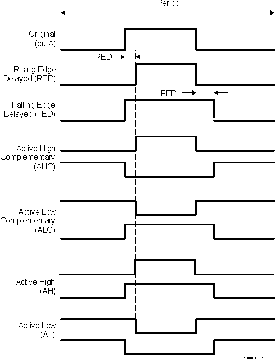 Figure 29-34 Dead-Band Waveforms for Typical Cases (0% < Duty < 100%)
The dead-band submodule supports independent values for rising-edge (RED) and falling-edge (FED) delays. The amount of delay is programmed using the EPWM_DBRED and EPWM_DBFED registers. These are 10-bit registers and their value represents the number of time-base clock, TBCLK, periods a signal edge is delayed by. For example, the formula to calculate falling-edge-delay and rising-edge-delay are:
FED = EPWM_DBFED × TTBCLK
RED = EPWM_DBRED × TTBCLK
Where TTBCLK is the period of TBCLK, the prescaled version of SYSCLKOUT.
29.2.28 PWM-Chopper (PC) Submodule
Figure 29-35 illustrates the PWM-chopper (PC) submodule within the ePWM module. The PWM-chopper submodule allows a high-frequency carrier signal to modulate the PWM waveform generated by the action-qualifier and dead-band submodules. This capability is important if you need pulse transformer-based gate drivers to control the power switching elements.
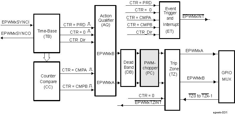 Figure 29-35 PWM-Chopper Submodule
29.2.29 Purpose of the PWM-Chopper Submodule
The key functions of the PWM-chopper submodule are:
- Programmable chopping (carrier) frequency
- Programmable pulse width of first pulse
- Programmable duty cycle of second and subsequent pulses
- Can be fully bypassed if not required
29.2.30 Controlling the PWM-Chopper Submodule
The PWM-chopper submodule operation is controlled via the register in Table 29-40.
| Acronym | Register Description | Address Offset | Shadowed |
|---|---|---|---|
| EPWM_PCCTL | PWM-chopper Control Register | 3Ch | No |
29.2.31 Operational Highlights for the PWM-Chopper Submodule
Figure 29-36 shows the operational details of the PWM-chopper submodule. The carrier clock is derived from SYSCLKOUT. Its frequency and duty cycle are controlled via the CHPFREQ and CHPDUTY bits in the EPWM_PCCTL register. The one-shot block is a feature that provides a high energy first pulse to ensure hard and fast power switch turn on, while the subsequent pulses sustain pulses, ensuring the power switch remains on. The one-shot width is programmed via the OSHTWTH bits. The PWM-chopper submodule can be fully disabled (bypassed) via the CHPEN bit.
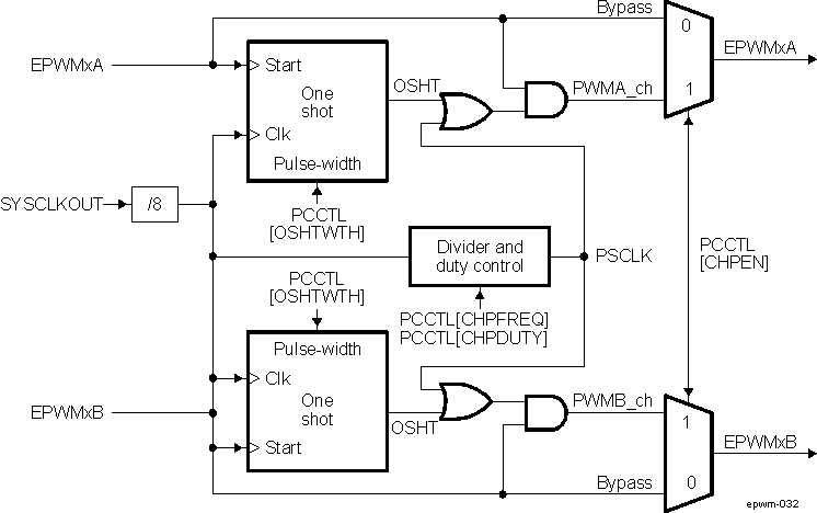 Figure 29-36 PWM-Chopper Submodule Signals and Registers
29.2.32 PWM Chopper Waveforms
Figure 29-37 shows simplified waveforms of the chopping action only; one-shot and duty-cycle control are not shown. Details of the one-shot and duty-cycle control are discussed in the following sections.
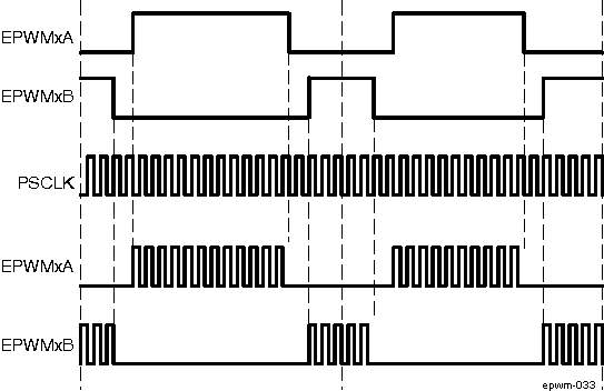 Figure 29-37 Simple PWM-Chopper Submodule Waveforms Showing Chopping Action Only
29.2.33 PWM-Chopper One-Shot Pulse
The width of the first pulse can be programmed to any of 16 possible pulse width values. The width or period of the first pulse is given by:
T1stpulse = TSYSCLKOUT × 8 × OSHTWTH
Where TSYSCLKOUT is the period of the system clock (SYSCLKOUT) and OSHTWTH is the four control bits (value from 1 to 16)
Figure 29-38 shows the first and subsequent sustaining pulses.
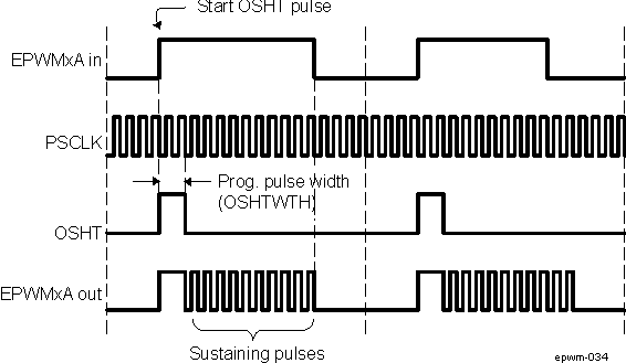 Figure 29-38 PWM-Chopper Submodule Waveforms Showing the First Pulse and
Subsequent Sustaining Pulses
29.2.34 PWM-Chopper Duty Cycle Control
Pulse transformer-based gate drive designs need to comprehend the magnetic properties or characteristics of the transformer and associated circuitry. Saturation is one such consideration. To assist the gate drive designer, the duty cycles of the second and subsequent pulses have been made programmable. These sustaining pulses ensure the correct drive strength and polarity is maintained on the power switch gate during the on period, and hence a programmable duty cycle allows a design to be tuned or optimized via software control.
Figure 29-39 shows the duty cycle control that is possible by programming the CHPDUTY bits. One of seven possible duty ratios can be selected ranging from 12.5% to 87.5%.
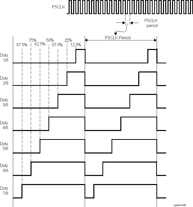 Figure 29-39 PWM-Chopper Submodule Waveforms Showing the Pulse Width (Duty Cycle) Control of Sustaining Pulses
29.2.35 ePWM Trip-Zone (TZ) Submodule
Figure 29-40 shows how the trip-zone (TZ) submodule fits within the ePWM module. Each ePWM module is connected to every TZ signal that are sourced from the GPIO MUX. These signals indicates external fault or trip conditions, and the ePWM outputs can be programmed to respond accordingly when faults occur. See Section 29.1.3 to determine the number of trip-zone pins available for the device.
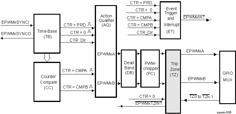 Figure 29-40 ePWM Trip-Zone Submodule
29.2.36 Purpose of the ePWM Trip-Zone Submodule
The key functions of the trip-zone submodule are:
- Trip inputs TZ0 to TZk-1 can be flexibly mapped to any ePWM module.
- Upon a fault condition, outputs EPWMxA and EPWMxB can be forced to one of the following:
- High
- Low
- High-impedance
- No action taken
- Support for one-shot trip (OSHT) for major short circuits or over-current conditions.
- Support for cycle-by-cycle tripping (CBC) for current limiting operation.
- Each trip-zone input pin can be allocated to either one-shot or cycle-by-cycle operation.
- Interrupt generation is possible on any trip-zone pin.
- Software-forced tripping is also supported.
- The trip-zone submodule can be fully bypassed if it is not required.
For each ePWMx, from the tripzone inputs EPWM_TRIP_TZ[5:0], ONLY the EPWM_TRIP_TZ[0] input of ePWM tripzone is chip accessible and usable, i.e. k=1.
29.2.37 Controlling and Monitoring the ePWM Trip-Zone Submodule
The trip-zone submodule operation is controlled and monitored through the following registers:
| Acronym | Register Description | Address Offset | Shadowed |
|---|---|---|---|
| EPWM_TZSEL | Trip-Zone Select Register | 24h | No |
| EPWM_TZCTL | Trip-Zone Control Register | 28h | No |
| EPWM_TZEINT | Trip-Zone Enable Interrupt Register | 2Ah | No |
| EPWM_TZFLG | Trip-Zone Flag Register | 2Ch | No |
| EPWM_TZCLR | Trip-Zone Clear Register | 2Eh | No |
| EPWM_TZFRC | Trip-Zone Force Register | 30h | No |
29.2.38 Operational Highlights for the ePWM Trip-Zone Submodule
The following sections describe the operational highlights and configuration options for the trip-zone submodule.
The trip-zone signals at pin TZ0 to TZk-1 is an active-low input signal. When the pin goes low, it indicates that a trip event has occurred. Each ePWM module can be individually configured to ignore or use each of the trip-zone pins. Which trip-zone pins are used by a particular ePWM module is determined by the EPWM_TZSEL register for that specific ePWM module. The trip-zone signal may or may not be synchronized to the system clock (SYSCLKOUT). A minimum of 1 SYSCLKOUT low pulse on the TZn inputs is sufficient to trigger a fault condition in the ePWM module. The asynchronous trip makes sure that if clocks are missing for any reason, the outputs can still be tripped by a valid event present on the TZk inputs.
Only the TZ[0] input is accessible at chip level (i.e. k=1).
The TZk input can be individually configured to provide either a cycle-by-cycle or one-shot trip event for a ePWM module. The configuration is determined by the EPWM_TZSEL[7:0] CBCk and EPWM_TZSEL[15:8] OSHTk bits (where k corresponds to the trip pin) respectively.
- Cycle-by-Cycle (CBC): When a cycle-by-cycle trip event occurs, the action specified in the EPWM_TZCTL register is carried out immediately on the EPWMxA and/or EPWMxB output. Table 29-42 lists the possible actions. In addition, the cycle-by-cycle trip event flag (EPWM_TZFLG[1] CBC) is set and a EPWMxTZINT interrupt is generated if it is enabled in the EPWM_TZEINT register.
The specified condition on the pins is automatically cleared when the ePWM time-base counter reaches zero (EPWM_TBCNT bitfield TBCNT = 0000h) if the trip event is no longer present. Therefore, in this mode, the trip event is cleared or reset every PWM cycle. The EPWM_TZFLG[1] CBC flag bit will remain set until it is manually cleared by writing to the EPWM_TZCLR[1] CBC bit. If the cycle-by-cycle trip event is still present when the EPWM_TZFLG[1] CBC bit is cleared, then it will again be immediately set.
- One-Shot (OSHT): When a one-shot trip event occurs, the action specified in the EPWM_TZCTL register is carried out immediately on the EPWMxA and/or EPWMxB output. Table 29-42 lists the possible actions. In addition, the one-shot trip event flag (EPWM_TZFLG[2] OST) is set and a EPWMxTZINT interrupt is generated if it is enabled in the EPWM_TZEINT register. The one-shot trip condition must be cleared manually by writing to the EPWM_TZCLR[2] OST bit.
The action taken when a trip event occurs can be configured individually for each of the ePWM output pins by way of the EPWM_TZCTL[1:0] TZA and EPWM_TZCTL[3:2] TZB register bits. One of four possible actions, shown in Table 29-42, can be taken on a trip event.
| EPWM_TZCTL[1:0] TZA and/or EPWM_TZCTL[3:2] TZB | EPWMxA and/or EPWMxB | Comment |
|---|---|---|
| 0 | High-Impedance | Tripped |
| 1h | Force to High State | Tripped |
| 2h | Force to Low State | Tripped |
| 3h | No Change | Do Nothing. No change is made to the output. |
29.2.39 ePWM Trip-Zone Configurations
Scenario A:
A one-shot trip event on
TZ0 pulls both EPWM1A, EPWM1B low and also forces EPWM2A and EPWM2B high.
- Configure the ePWM1 registers as follows:
- EPWM_TZSEL[8] OSHT1 = 1: enables TZ as a one-shot event source for ePWM1
- EPWM_TZCTL[1:0] TZA = 2: EPWM1A will be forced low on a trip event.
- EPWM_TZCTL[3:2] TZB = 2: EPWM1B will be forced low on a trip event.
- Configure the ePWM2 registers as follows:
- EPWM_TZSEL[8] OSHT1 = 1: enables TZ as a one-shot event source for ePWM2
- EPWM_TZCTL[1:0] TZA = 1: EPWM2A will be forced high on a trip event.
- EPWM_TZCTL[3:2] TZB = 1: EPWM2B will be forced high on a trip event.
29.2.40 Generating ePWM Trip Event Interrupts
Figure 29-41 and Figure 29-42 illustrate the trip-zone submodule control and interrupt logic, respectively.
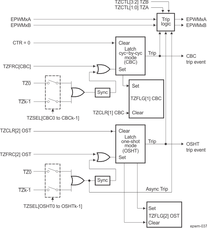 Figure 29-41 ePWM Trip-Zone Submodule Mode Control Logic
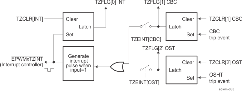 Figure 29-42 ePWM Trip-Zone Submodule Interrupt Logic
29.2.41 ePWM Event-Trigger (ET) Submodule
Figure 29-43 shows the event-trigger (ET) submodule in the ePWM system. The event-trigger submodule manages the events generated by the time-base submodule and the counter-compare submodule to generate an aggregated interrupt request.
The ePWMx ET interrupt request output is further routed via the device IRQ_CROSSBAR, to different device host interrupt controllers, located outside PWMSSn. For more details on interrupt event routing outside the ePWM, refer to the Section 29.1.3.
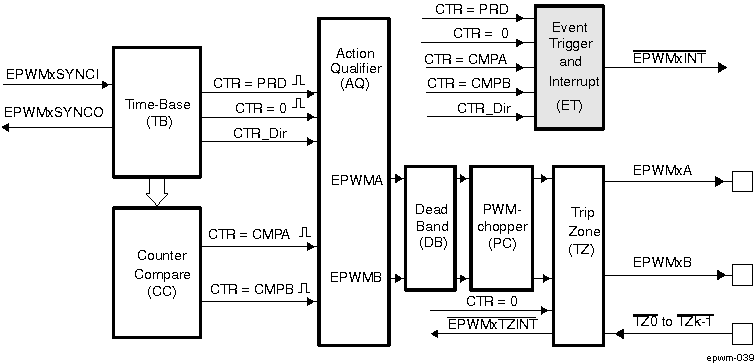 Figure 29-43 ePWM Event-Trigger Submodule
29.2.42 Purpose of the ePWM Event-Trigger Submodule
The key functions of the event-trigger submodule are:
- Receives event inputs generated by the time-base and counter-compare submodules
- Uses the time-base direction information for up/down event qualification
- Uses prescaling logic to issue interrupt requests at:
- Every event
- Every second event
- Every third event
- Provides full visibility of event generation via event counters and flags
29.2.43 Controlling and Monitoring the ePWM Event-Trigger Submodule
The key registers used to configure the event-trigger submodule are shown in Table 29-43:
| Acronym | Register Description | Address Offset | Shadowed |
|---|---|---|---|
| EPWM_ETSEL | Event-Trigger Selection Register | 32h | No |
| EPWM_ETPS | Event-Trigger Prescale Register | 34h | No |
| EPWM_ETFLG | Event-Trigger Flag Register | 36h | No |
| EPWM_ETCLR | Event-Trigger Clear Register | 38h | No |
| EPWM_ETFRC | Event-Trigger Force Register | 3Ah | No |
29.2.44 Operational Overview of the ePWM Event-Trigger Submodule
The following sections describe the event-trigger submodule's operational highlights.
Each ePWM module has one interrupt request line as shown in Figure 29-44. Mapping interrupt lines to device host interrupt controllers is device specific and is covered in the Section 29.1.3.
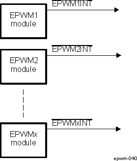 Figure 29-44 ePWM Event-Trigger Submodule Inter-Connectivity to Interrupt Controller
The event-trigger submodule monitors various event conditions (the left side inputs to event-trigger submodule shown in Figure 29-45) and can be configured to prescale these events before issuing an Interrupt request. The event-trigger prescaling logic can issue Interrupt requests at:
- Every event
- Every second event
- Every third event
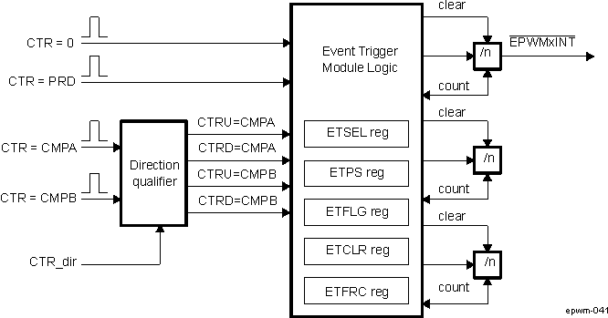 Figure 29-45 ePWM Event-Trigger Submodule Showing Event Inputs and Prescaled Outputs
- ETSEL—This selects which of the possible events will trigger an interrupt.
- ETPS—This programs the event prescaling options previously mentioned.
- ETFLG—These are flag bits indicating status of the selected and prescaled events.
- ETCLR—These bits allow you to clear the flag bits in the EPWM_ETFLG register via software.
- ETFRC—These bits allow software forcing of an event. Useful for debugging or software intervention.
A more detailed look at how the various register bits interact with the Interrupt is shown in Figure 29-46.
Figure 29-46 shows the event-trigger's interrupt generation logic. The interrupt-period (EPWM_ETPS[1:0] INTPRD) bits specify the number of events required to cause an interrupt pulse to be generated. The choices available are:
- Do not generate an interrupt
- Generate an interrupt on every event
- Generate an interrupt on every second event
- Generate an interrupt on every third event
An interrupt cannot be generated on every fourth or more events.
Which event can cause an interrupt is configured by the interrupt selection (EPWM_ETSEL[2:0] INTSEL) bits. The event can be one of the following:
- Time-base counter equal to zero (EPWM_TBCNT bitfield TBCNT = 0000h).
- Time-base counter equal to period (EPWM_TBCNT bitfield TBCNT = TBPRD value in EPWM_TBPRD active register).
- Time-base counter equal to the compare A register (EPWM_CMPA) when the timer is incrementing.
- Time-base counter equal to the compare A register (EPWM_CMPA) when the timer is decrementing.
- Time-base counter equal to the compare B register (EPWM_CMPB) when the timer is incrementing.
- Time-base counter equal to the compare B register (EPWM_CMPB) when the timer is decrementing.
The number of events that have occurred can be read from the interrupt event counter (EPWM_ETPS[3:2] INTCNT) register bits. That is, when the specified event occurs the EPWM_ETPS[3:2] INTCNT bits are incremented until they reach the value specified by EPWM_ETPS[1:0] INTPRD. When EPWM_ETPS[3:2] INTCNT = EPWM_ETPS[1:0] INTPRD the counter stops counting and its output is set. The counter is only cleared when an interrupt is sent to the interrupt controller.
When EPWM_ETPS[3:2] INTCNT reaches EPWM_ETPS[1:0] INTPRD, one of the following behaviors will occur:
- If interrupts are enabled, EPWM_ETSEL[3] INTEN = 1 and the interrupt flag is clear, EPWM_ETFLG[0] INT = 0, then an interrupt pulse is generated and the interrupt flag is set, EPWM_ETFLG[0] INT = 1, and the event counter is cleared EPWM_ETPS[3:2] INTCNT = 0. The counter will begin counting events again.
- If interrupts are disabled, EPWM_ETSEL[3] INTEN = 0, or the interrupt flag is set, EPWM_ETFLG[0] INT = 1, the counter stops counting events when it reaches the period value EPWM_ETPS[3:2] INTCNT = EPWM_ETPS[1:0] INTPRD.
- If interrupts are enabled, but the interrupt flag is already set, then the counter will hold its output high until the ENTFLG[0] INT flag is cleared. This allows for one interrupt to be pending while one is serviced.
Writing to the INTPRD bits will automatically clear the counter INTCNT = 0 and the counter output will be reset (so no interrupts are generated). Writing a 1 to the EPWM_ETFRC[0] INT bit will increment the event counter INTCNT. The counter will behave as described above when INTCNT = INTPRD. When INTPRD = 0, the counter is disabled and hence no events will be detected and the EPWM_ETFRC[0] INT bit is also ignored.
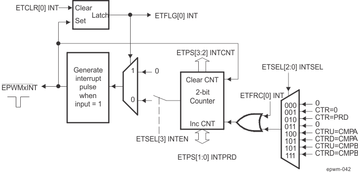 Figure 29-46 ePWM Event-Trigger Interrupt Generator
29.2.45 High-Resolution PWM (HRPWM) Submodule
Figure 29-47 shows the high-resolution PWM (HRPWM) submodule in the ePWM system. Some devices include the high-resolution PWM submodule, see Section 29.1.3 to determine which ePWM instances include this feature.
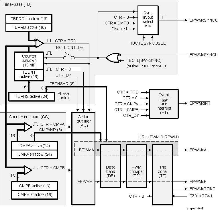 Figure 29-47 HRPWM System Interface
29.2.46 Purpose of the High-Resolution PWM Submodule
The enhanced high-resolution pulse-width modulator (eHRPWM) extends the time resolution capabilities of the conventionally derived digital pulse-width modulator (PWM). HRPWM is typically used when PWM resolution falls below ~9-10 bits. The key features of HRPWM are:
- Extended time resolution capability
- Used in both duty cycle and phase-shift control methods
- Finer time granularity control or edge positioning using extensions to the Compare A and Phase registers
- Implemented using the A signal path of PWM, that is, on the EPWMxA output. EPWMxB output has conventional PWM capabilities
The ePWM peripheral is used to perform a function that is mathematically equivalent to a digital-to-analog converter (DAC). As shown in Figure 29-48, the effective resolution for conventionally generated PWM is a function of PWM frequency (or period) and system clock frequency.
 Figure 29-48 Resolution Calculations for Conventionally Generated PWM
If the required PWM operating frequency does not offer sufficient resolution in PWM mode, you may want to consider HRPWM. As an example of improved performance offered by HRPWM, Table 29-44 shows resolution in bits for various PWM frequencies. Table 29-44 values assume a MEP step size of 180 ps. See your device-specific data manual for typical and maximum performance specifications for the MEP.
| PWM Frequency (kHz) | Regular Resolution (PWM) | High Resolution (HRPWM) | |||
|---|---|---|---|---|---|
| Bits | % | Bits | % | ||
| 20 | 12.3 | 0.0 | 18.1 | 0.000 | |
| 50 | 11.0 | 0.0 | 16.8 | 0.001 | |
| 100 | 10.0 | 0.1 | 15.8 | 0.002 | |
| 150 | 9.4 | 0.2 | 15.2 | 0.003 | |
| 200 | 9.0 | 0.2 | 14.8 | 0.004 | |
| 250 | 8.6 | 0.3 | 14.4 | 0.005 | |
| 500 | 7.6 | 0.5 | 13.8 | 0.007 | |
| 1000 | 6.6 | 1.0 | 12.4 | 0.018 | |
| 1500 | 6.1 | 1.5 | 11.9 | 0.027 | |
| 2000 | 5.6 | 2.0 | 11.4 | 0.036 | |
Although each application may differ, typical low-frequency PWM operation (below 250 kHz) may not require HRPWM. HRPWM capability is most useful for high-frequency PWM requirements of power conversion topologies such as:
- Single-phase buck, boost, and flyback
- Multi-phase buck, boost, and flyback
- Phase-shifted full bridge
- Direct modulation of D-Class power amplifiers
29.2.47 Architecture of the High-Resolution PWM Submodule
The HRPWM is based on micro edge positioner (MEP) technology. MEP logic is capable of positioning an edge very finely by sub-dividing one coarse system clock of a conventional PWM generator. The time step accuracy is on the order of 150 ps. The HRPWM also has a self-check software diagnostics mode to check if the MEP logic is running optimally, under all operating conditions.
Figure 29-49 shows the relationship between one coarse system clock and edge position in terms of MEP steps, which are controlled via an 8-bit field in the Compare A extension register (HRPWM_CMPAHR).
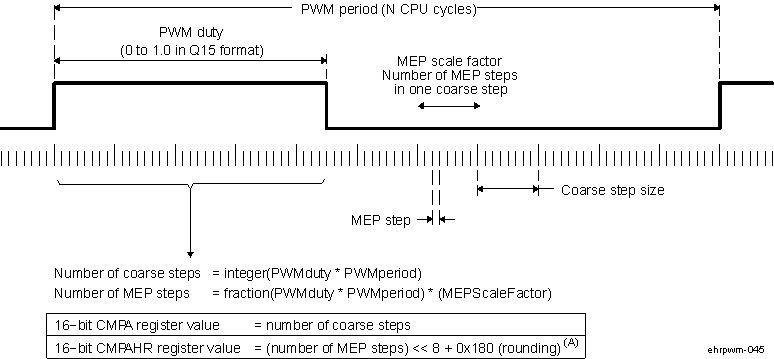
To generate an HRPWM waveform, configure the TBM, CCM, and AQM registers as you would to generate a conventional PWM of a given frequency and polarity. The HRPWM works together with the TBM, CCM, and AQM registers to extend edge resolution, and should be configured accordingly. Although many programming combinations are possible, only a few are needed and practical.
29.2.48 Controlling and Monitoring the High-Resolution PWM Submodule
The MEP of the HRPWM is controlled by two extension registers, each 8-bits wide. These two HRPWM registers are concatenated with the 16-bit EPWM_TBPHS and EPWM_CMPA registers used to control PWM operation.
- HRPWM_TBPHSHR - Time-Base Phase High-Resolution Register
- HRPWM_CMPAHR - Counter-Compare A High-Resolution Register
Table 29-45 lists the registers used to control and monitor the high-resolution PWM submodule.
| Acronym | Register Description | Address Offset | Shadowed |
|---|---|---|---|
| HRPWM_TBPHSHR | Extension Register for HRPWM Phase | 4h | No |
| HRPWM_CMPAHR | Extension Register for HRPWM Duty | 10h | Yes |
| HRPWM_HRCTL | HRPWM Configuration Register | 1040h | No |
29.2.49 Configuring the High-Resolution PWM Submodule
Once the ePWM has been configured to provide conventional PWM of a given frequency and polarity, the HRPWM is configured by programming the HRPWM_HRCTL register located at offset address 1040h. This register provides configuration options for the following key operating modes:
- Edge Mode: The MEP can be programmed to provide precise position control on the rising edge (RE), falling edge (FE), or both edges (BE) at the same time. FE and RE are used for power topologies requiring duty cycle control, while BE is used for topologies requiring phase shifting, for example, phase shifted full bridge.
- Control Mode: The MEP is programmed to be controlled either from the HRPWM_CMPAHR register (duty cycle control) or the HRPWM_TBPHSHR register (phase control). RE or FE control mode should be used with HRPWM_CMPAHR register. BE control mode should be used with HRPWM_TBPHSHR register.
- Shadow Mode: This mode provides the same shadowing (double buffering) option as in regular PWM mode. This option is valid only when operating from the HRPWM_CMPAHR register and should be chosen to be the same as the regular load option for the CMPA register. If HRPWM_TBPHSHR is used, then this option has no effect.
29.2.50 Operational Highlights for the High-Resolution PWM Submodule
The MEP logic is capable of placing an edge in one of 255 (8 bits) discrete time steps, each of which has a time resolution on the order of 150 ps. The MEP works with the TBM and CCM registers to be certain that time steps are optimally applied and that edge placement accuracy is maintained over a wide range of PWM frequencies, system clock frequencies and other operating conditions. Table 29-46 shows the typical range of operating frequencies supported by the HRPWM.
| System (MHz) | MEP Steps Per SYSCLKOUT(1) (2) (3) | PWM Minimum (Hz)(4) | PWM Maximum (MHz) | Resolution at Maximum (Bits)(5) |
|---|---|---|---|---|
| 50.0 | 111 | 763 | 2.50 | 11.1 |
| 60.0 | 93 | 916 | 3.00 | 10.9 |
| 70.0 | 79 | 1068 | 3.50 | 10.6 |
| 80.0 | 69 | 1221 | 4.00 | 10.4 |
| 90.0 | 62 | 1373 | 4.50 | 10.3 |
| 100.0 | 56 | 1526 | 5.00 | 10.1 |
29.2.51 HRPWM Edge Positioning
In a typical power control loop (switch modes, digital motor control (DMC), uninterruptible power supply (UPS)), a digital controller (PID, 2pole/2zero, lag/lead, etc.) issues a duty command, usually expressed in a per unit or percentage terms.
In the following example, assume that for a particular operating point, the demanded duty cycle is 0.405 or 40.5% on-time and the required converter PWM frequency is 1.25 MHz. In conventional PWM generation with a system clock of 100 MHz, the duty cycle choices are in the vicinity of 40.5%. In Figure 29-50, a compare value of 32 counts (duty = 40%) is the closest to 40.5% that you can attain. This is equivalent to an edge position of 320 ns instead of the desired 324 ns. This data is shown in Table 29-47.
By utilizing the MEP, you can achieve an edge position much closer to the desired point of 324 ns. Table 29-47 shows that in addition to the CMPA value, 22 steps of the MEP (HRPWM_CMPAHR register) will position the edge at 323.96 ns, resulting in almost zero error. In this example, it is assumed that the MEP has a step resolution of 180 ns.
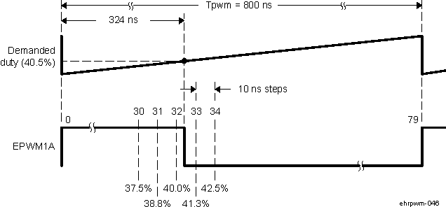 Figure 29-50 Required PWM Waveform for a Requested Duty = 40.5%
| CMPA (count)(1) (2) (3) | DUTY (%) | High Time (ns) | CMPA (count) | CMPAHR (count) | Duty (%) | High Time (ns) | |
|---|---|---|---|---|---|---|---|
| 28 | 35.0 | 280 | 32 | 18 | 40.405 | 323.24 | |
| 29 | 36.3 | 290 | 32 | 19 | 40.428 | 323.42 | |
| 30 | 37.5 | 300 | 32 | 20 | 40.450 | 323.60 | |
| 31 | 38.8 | 310 | 32 | 21 | 40.473 | 323.78 | |
| 32 | 40.0 | 320 | 32 | 22 | 40.495 | 323.96 | |
| 33 | 41.3 | 330 | 32 | 23 | 40.518 | 324.14 | |
| 34 | 42.5 | 340 | 32 | 24 | 40.540 | 324.32 | |
| 32 | 25 | 40.563 | 324.50 | ||||
| Required | 32 | 26 | 40.585 | 324.68 | |||
| 32.40 | 40.5 | 324 | 32 | 27 | 40.608 | 324.86 |
29.2.52 HRPWM Scaling Considerations
The mechanics of how to position an edge precisely in time has been demonstrated using the resources of the standard (EPWM_CMPA) and MEP (HRPWM_CMPAHR) registers. In a practical application, however, it is necessary to seamlessly provide the CPU a mapping function from a per-unit (fractional) duty cycle to a final integer (non-fractional) representation that is written to the [CMPA:CMPAHR] register combination.
To do this, first examine the scaling or mapping steps involved. It is common in control software to express duty cycle in a per-unit or percentage basis. This has the advantage of performing all needed math calculations without concern for the final absolute duty cycle, expressed in clock counts or high time in ns. Furthermore, it makes the code more transportable across multiple converter types running different PWM frequencies.
To implement the mapping scheme, a two-step scaling procedure is required.
Assumptions for this example:
| System clock, SYSCLKOUT | = | 10 ns (100 MHz) |
| PWM frequency | = | 1.25 MHz (1/800 ns) |
| Required PWM duty cycle, PWMDuty | = | 0.405 (40.5%) |
| PWM period in terms of coarse steps, PWMperiod (800 ns/10 ns) | = | 80 |
| Number of MEP steps per coarse step at 180 ps (10 ns/180 ps), MEP_SF | = | 55 |
| Value to keep CMPAHR within the range of 1-255 and fractional rounding constant (default value) | = | 180h |
Step 1: Percentage Integer Duty value conversion for EPWM_CMPA register
| EPWM_CMPA register value | = | int(PWMDuty × PWMperiod); int means integer part |
| = | int(0.405 × 80) | |
| = | int(32.4) | |
| EPWM_CMPA register value | = | 32 (20h) |
Step 2: Fractional value conversion for HRPWM_CMPAHR register
| HRPWM_CMPAHR register value | = | (frac(PWMDuty × PWMperiod) × MEP_SF) << 8) + 180h; frac means fractional part |
| = | (frac(32.4) × 55 <<8) + 180h; Shift is to move the value as CMPAHR high byte | |
| = | ((0.4 × 55) <<8) + 180h | |
| = | (22 <<8) + 180h | |
| = | 22 × 256 + 180h ; Shifting left by 8 is the same multiplying by 256. | |
| = | 5632 + 180h | |
| = | 1600h + 180h | |
| HRPWM_CMPAHR value | = | 1780h; HRPWM_CMPAHR value = 1700h, lower 8 bits will be ignored by hardware. |
29.2.53 HRPWM Duty Cycle Range Limitation
In high resolution mode, the MEP is not active for 100% of the PWM period. It becomes operational 3 SYSCLKOUT cycles after the period starts.
Duty cycle range limitations are illustrated in Figure 29-51. This limitation imposes a lower duty cycle limit on the MEP. For example, precision edge control is not available all the way down to 0% duty cycle. Although for the first 3 or 6 cycles, the HRPWM capabilities are not available, regular PWM duty control is still fully operational down to 0% duty. In most applications this should not be an issue as the controller regulation point is usually not designed to be close to 0% duty cycle.
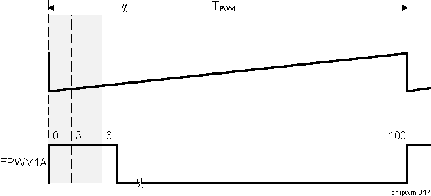 Figure 29-51 Low % Duty Cycle Range Limitation Example When PWM Frequency = 1 MHz
If the application demands HRPWM operation in the low percent duty cycle region, then the HRPWM can be configured to operate in count-down mode with the rising edge position (REP) controlled by the MEP. This is illustrated in Figure 29-52. In this case low percent duty limitation is no longer an issue.
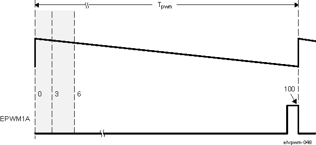 Figure 29-52 High % Duty Cycle Range Limitation Example when PWM Frequency = 1 MHz
29.2.54 eHRPWM Functional Register Groups
The Table 29-48 lists the groups of ePWM and the high-resolution PWM module registers according to their functionalities.
| Register Name | Offset | Size (×16) | Shadow | Register Description |
|---|---|---|---|---|
| Time-Base Submodule Registers | ||||
| EPWM_TBCTL | 0h | 1 | No | Time-Base Control Register |
| EPWM_TBSTS | 2h | 1 | No | Time-Base Status Register |
| EPWM_TBPHS | 6h | 1 | No | Time-Base Phase Register |
| EPWM_TBCNT | 8h | 1 | No | Time-Base Counter Register |
| EPWM_TBPRD | Ah | 1 | Yes | Time-Base Period Register |
| Counter-Compare Submodule Registers | ||||
| EPWM_CMPCTL | Eh | 1 | No | Counter-Compare Control Register |
| EPWM_CMPA | 12h | 1 | Yes | Counter-Compare A Register |
| EPWM_CMPB | 14h | 1 | Yes | Counter-Compare B Register |
| Action-Qualifier Submodule Registers | ||||
| EPWM_AQCTLA | 16h | 1 | No | Action-Qualifier Control Register for Output A (EPWMxA) |
| EPWM_AQCTLB | 18h | 1 | No | Action-Qualifier Control Register for Output B (EPWMxB) |
| EPWM_AQSFRC | 1Ah | 1 | No | Action-Qualifier Software Force Register |
| EPWM_AQCSFRC | 1Ch | 1 | Yes | Action-Qualifier Continuous S/W Force Register Set |
| Dead-Band Generator Submodule Registers | ||||
| EPWM_DBCTL | 1Eh | 1 | No | Dead-Band Generator Control Register |
| EPWM_DBRED | 20h | 1 | No | Dead-Band Generator Rising Edge Delay Count Register |
| EPWM_DBFED | 22h | 1 | No | Dead-Band Generator Falling Edge Delay Count Register |
| Trip-Zone Submodule Registers | ||||
| EPWM_TZSEL | 24h | 1 | No | Trip-Zone Select Register |
| EPWM_TZCTL | 28h | 1 | No | Trip-Zone Control Register |
| EPWM_TZEINT | 2Ah | 1 | No | Trip-Zone Enable Interrupt Register |
| EPWM_TZFLG | 2Ch | 1 | No | Trip-Zone Flag Register |
| EPWM_TZCLR | 2Eh | 1 | No | Trip-Zone Clear Register |
| EPWM_TZFRC | 30h | 1 | No | Trip-Zone Force Register |
| Event-Trigger Submodule Registers | ||||
| EPWM_ETSEL | 32h | 1 | No | Event-Trigger Selection Register |
| EPWM_ETPS | 34h | 1 | No | Event-Trigger Pre-Scale Register |
| EPWM_ETFLG | 36h | 1 | No | Event-Trigger Flag Register |
| EPWM_ETCLR | 38h | 1 | No | Event-Trigger Clear Register |
| EPWM_ETFRC | 3Ah | 1 | No | Event-Trigger Force Register |
| PWM-Chopper Submodule Registers | ||||
| EPWM_PCCTL | 3Ch | 1 | No | PWM-Chopper Control Register |
| High-Resolution PWM (HRPWM) Submodule Registers | ||||
| HRPWM_TBPHSHR | 4h | 1 | No | Extension for HRPWM Phase Register |
| HRPWM_CMPAHR | 10h | 1 | No | Extension for HRPWM Counter-Compare A Register |
| HRPWM_HRCTL | 40h | 1 | No | HRPWM Control Register |
29.2.55 PWMSS_EPWM Register Manual
This section provides description of the device PWMSS ePWM and High Resolution-PWM relevant functional registers.
29.2.56 PWMSS_EPWM Instance Summary
| Module Name | Module Base Address L4_PER2 Interconnect | Size (Bytes) |
|---|---|---|
| PWMSS1_EPWM | 0x4843 E200 | 136 Bytes |
| PWMSS2_EPWM | 0x4844 0200 | 136 Bytes |
| PWMSS3_EPWM | 0x4844 2200 | 136 Bytes |
29.2.57 PWMSS_EPWM Registers
29.2.58 PWMSS_EPWM Register Summary
| Register Name | Type | Register Width (Bits) | Address Offset | PWMSS1_EPWM Physical Address L4_PER2 Interconnect | PWMSS2_EPWM Physical Address L4_PER2 Interconnect | PWMSS3_EPWM Physical Address L4_PER2 Interconnect |
|---|---|---|---|---|---|---|
| EPWM_TBCTL | RW | 16 | 0x0000 0000 | 0x4843 E200 | 0x4844 0200 | 0x4844 2200 |
| EPWM_TBSTS | RW | 16 | 0x0000 0002 | 0x4843 E202 | 0x4844 0202 | 0x4844 2202 |
| HRPWM_TBPHSHR | RW | 16 | 0x0000 0004 | 0x4843 E204 | 0x4844 0204 | 0x4844 2204 |
| EPWM_TBPHS | RW | 16 | 0x0000 0006 | 0x4843 E206 | 0x4844 0206 | 0x4844 2206 |
| EPWM_TBCNT | RW | 16 | 0x0000 0008 | 0x4843 E208 | 0x4844 0208 | 0x4844 2208 |
| EPWM_TBPRD | RW | 16 | 0x0000 000A | 0x4843 E20A | 0x4844 020A | 0x4844 220A |
| EPWM_CMPCTL | RW | 16 | 0x0000 000E | 0x4843 E20E | 0x4844 020E | 0x4844 220E |
| HRPWM_CMPAHR | RW | 16 | 0x0000 0010 | 0x4843 E210 | 0x4844 0210 | 0x4844 2210 |
| EPWM_CMPA | RW | 16 | 0x0000 0012 | 0x4843 E212 | 0x4844 0212 | 0x4844 2212 |
| EPWM_CMPB | RW | 16 | 0x0000 0014 | 0x4843 E214 | 0x4844 0214 | 0x4844 2214 |
| EPWM_AQCTLA | RW | 16 | 0x0000 0016 | 0x4843 E216 | 0x4844 0216 | 0x4844 2216 |
| EPWM_AQCTLB | RW | 16 | 0x0000 0018 | 0x4843 E218 | 0x4844 0218 | 0x4844 2218 |
| EPWM_AQSFRC | RW | 16 | 0x0000 001A | 0x4843 E21A | 0x4844 021A | 0x4844 221A |
| EPWM_AQCSFRC | RW | 16 | 0x0000 001C | 0x4843 E21C | 0x4844 021C | 0x4844 221C |
| EPWM_DBCTL | RW | 16 | 0x0000 001E | 0x4843 E21E | 0x4844 021E | 0x4844 221E |
| EPWM_DBRED | RW | 16 | 0x0000 0020 | 0x4843 E220 | 0x4844 0220 | 0x4844 2220 |
| EPWM_DBFED | RW | 16 | 0x0000 0022 | 0x4843 E222 | 0x4844 0222 | 0x4844 2222 |
| EPWM_TZSEL | RW | 16 | 0x0000 0024 | 0x4843 E224 | 0x4844 0224 | 0x4844 2224 |
| EPWM_TZCTL | RW | 16 | 0x0000 0028 | 0x4843 E228 | 0x4844 0228 | 0x4844 2228 |
| EPWM_TZEINT | RW | 16 | 0x0000 002A | 0x4843 E22A | 0x4844 022A | 0x4844 222A |
| EPWM_TZFLG | R | 16 | 0x0000 002C | 0x4843 E22C | 0x4844 022C | 0x4844 222C |
| EPWM_TZCLR | RW | 16 | 0x0000 002E | 0x4843 E22E | 0x4844 022E | 0x4844 222E |
| EPWM_TZFRC | RW | 16 | 0x0000 0030 | 0x4843 E230 | 0x4844 0230 | 0x4844 2230 |
| EPWM_ETSEL | RW | 16 | 0x0000 0032 | 0x4843 E232 | 0x4844 0232 | 0x4844 2232 |
| EPWM_ETPS | RW | 16 | 0x0000 0034 | 0x4843 E234 | 0x4844 0234 | 0x4844 2234 |
| EPWM_ETFLG | R | 16 | 0x0000 0036 | 0x4843 E236 | 0x4844 0236 | 0x4844 2236 |
| EPWM_ETCLR | RW | 16 | 0x0000 0038 | 0x4843 E238 | 0x4844 0238 | 0x4844 2238 |
| EPWM_ETFRC | RW | 16 | 0x0000 003A | 0x4843 E23A | 0x4844 023A | 0x4844 223A |
| EPWM_PCCTL | RW | 16 | 0x0000 003C | 0x4843 E23C | 0x4844 023C | 0x4844 223C |
| HRPWM_HRCTL | RW | 16 | 0x0000 00C0 | 0x4843 E2C0 | 0x4844 02C0 | 0x4844 22C0 |
29.2.59 PWMSS_EPWM Register Description
| Address Offset | 0x0000 0000 | ||
| Physical Address | 0x4843 E200 0x4844 0200 0x4844 2200 | Instance | PWMSS1_EPWM PWMSS2_EPWM PWMSS3_EPWM |
| Description | |||
| Type | RW | ||
| 15 | 14 | 13 | 12 | 11 | 10 | 9 | 8 | 7 | 6 | 5 | 4 | 3 | 2 | 1 | 0 |
| FREE_SOFT | PHSDIR | CLKDIV | var tiPageName = 'Literature reader-SPRUHZ7K-ja_JP'; var tiDocType = 'Technical Reference'; var tiLibraryStore = new com.TI.tiLibrary.tiLibraryStore(); var tiLibraryViewerStore = tiLibraryStore.viewer_store; RiotControl.addStore(tiLibraryStore); var subRoutes = riot.route.create(); subRoutes("/document-viewer/*/datasheet/*\\?*#*", function(gpn, url, params, anchor) { RiotControl.trigger("ti_library_open_viewer", { document: tiLibraryViewerStore.document, documentLocale: tiLibraryViewerStore.documentLocale, url: "/document-viewer/" + gpn + "/datasheet/" + url + "#" + anchor, toc: true, set_content: true }); }); subRoutes("/document-viewer/*/datasheet/*#*", function(gpn, url, anchor) { RiotControl.trigger("ti_library_open_viewer", { document: tiLibraryViewerStore.document, documentLocale: tiLibraryViewerStore.documentLocale, url: "/document-viewer/" + gpn + "/datasheet/" + url + "#" + anchor, toc: true, set_content: true }); }); subRoutes("/document-viewer/*/datasheet/*", function(gpn, url) { RiotControl.trigger("ti_library_open_viewer", { document: tiLibraryViewerStore.document, documentLocale: tiLibraryViewerStore.documentLocale, url: "/document-viewer/" + gpn + "/datasheet/" + url, toc: true, set_content: true }); }); subRoutes("/document-viewer/*/*/datasheet/*\\?*#*", function(locale, gpn, url, params, anchor) { RiotControl.trigger("ti_library_open_viewer", { document: tiLibraryViewerStore.document, documentLocale: tiLibraryViewerStore.documentLocale, url: "/document-viewer/" + locale + "/" + gpn + "/datasheet/" + url + "#" + anchor, toc: true, set_content: true }); }); subRoutes("/document-viewer/*/*/datasheet/*#*", function(locale, gpn, url, anchor) { RiotControl.trigger("ti_library_open_viewer", { document: tiLibraryViewerStore.document, documentLocale: tiLibraryViewerStore.documentLocale, url: "/document-viewer/" + locale + "/" + gpn + "/datasheet/" + url + "#" + anchor, toc: true, set_content: true }); }); subRoutes("/document-viewer/*/*/datasheet/*", function(locale, gpn, url) { RiotControl.trigger("ti_library_open_viewer", { document: tiLibraryViewerStore.document, documentLocale: tiLibraryViewerStore.documentLocale, url: "/document-viewer/" + locale + "/" + gpn + "/datasheet/" + url, toc: true, set_content: true }); }); subRoutes("/document-viewer/*/datasheet#*/*", function(gpn, url, fragment) { RiotControl.trigger("ti_library_open_viewer", { document: tiLibraryViewerStore.document, documentLocale: tiLibraryViewerStore.documentLocale, url: "/document-viewer/" + gpn + "/datasheet#" + url + "/" + fragment, toc: true, set_content: true }); }); subRoutes("/document-viewer/*/*/datasheet#*/*", function(locale, gpn, url, fragment) { RiotControl.trigger("ti_library_open_viewer", { document: tiLibraryViewerStore.document, documentLocale: tiLibraryViewerStore.documentLocale, url: "/document-viewer/" + locale + "/" + gpn + "/datasheet#" + url + "/" + fragment, toc: true, set_content: true }); }); subRoutes("/document-viewer/lit/html/*", function(litnum) { RiotControl.trigger("ti_library_open_viewer", { document: tiLibraryViewerStore.document, documentLocale: tiLibraryViewerStore.documentLocale, url: "/document-viewer/lit/html/" + litnum, toc: true, set_content: true }); }); subRoutes("/document-viewer/lit/html/*/*\\?*#*", function(litnum, url, params, anchor) { RiotControl.trigger("ti_library_open_viewer", { document: tiLibraryViewerStore.document, documentLocale: tiLibraryViewerStore.documentLocale, url: "/document-viewer/lit/html/" + litnum + "/" + url + "#" + anchor, toc: true, set_content: true }); }); subRoutes("/document-viewer/lit/html/*/*#*", function(litnum, url, anchor) { RiotControl.trigger("ti_library_open_viewer", { document: tiLibraryViewerStore.document, documentLocale: tiLibraryViewerStore.documentLocale, url: "/document-viewer/lit/html/" + litnum + "/" + url + "#" + anchor, toc: true, set_content: true }); }); subRoutes("/document-viewer/lit/html/*#*/*", function(litnum, url, anchor) { RiotControl.trigger("ti_library_open_viewer", { document: tiLibraryViewerStore.document, documentLocale: tiLibraryViewerStore.documentLocale, url: "/document-viewer/lit/html/" + litnum + "#" + url + "/" + anchor, toc: true, set_content: true }); }); subRoutes("/document-viewer/*/lit/html/*#*/*", function(locale, litnum, url, anchor) { RiotControl.trigger("ti_library_open_viewer", { document: tiLibraryViewerStore.document, documentLocale: tiLibraryViewerStore.documentLocale, url: "/document-viewer/" + locale + "/lit/html/" + litnum + "#" + url + "/" + anchor, toc: true, set_content: true }); }); subRoutes("/document-viewer/lit/html/*/*", function(litnum, url) { RiotControl.trigger("ti_library_open_viewer", { document: tiLibraryViewerStore.document, documentLocale: tiLibraryViewerStore.documentLocale, url: "/document-viewer/lit/html/" + litnum + "/" + url, toc: true, set_content: true }); }); subRoutes("/document-viewer/*/lit/html/*/*\\?*#*", function(locale, litnum, url, params, anchor) { RiotControl.trigger("ti_library_open_viewer", { document: tiLibraryViewerStore.document, documentLocale: tiLibraryViewerStore.documentLocale, url: "/document-viewer/" + locale + "/lit/html/" + litnum + "/" + url + "#" + anchor, toc: true, set_content: true }); }); subRoutes("/document-viewer/*/lit/html/*/*#*", function(locale, litnum, url, anchor) { RiotControl.trigger("ti_library_open_viewer", { document: tiLibraryViewerStore.document, documentLocale: tiLibraryViewerStore.documentLocale, url: "/document-viewer/" + locale + "/lit/html/" + litnum + "/" + url + "#" + anchor, toc: true, set_content: true }); }); subRoutes("/document-viewer/*/lit/html/*/*", function(locale, litnum, url) { RiotControl.trigger("ti_library_open_viewer", { document: tiLibraryViewerStore.document, documentLocale: tiLibraryViewerStore.documentLocale, url: "/document-viewer/" + locale + "/lit/html/" + litnum + "/" + url, toc: true, set_content: true }); }); var compose_url = function(q) { //URL format: scheme:[//[user[:password]@]host[:port]][/path][?query][#fragment] var tempUrl = q.url.replace("//www.ti.com/", ""); var url = tempUrl.replace("//www.ti.com/", ""); if (q.search != null) { var params = ""; var hash = ""; var url_parts = url.split('#'); if (url_parts.length == 2) { url = url_parts[0]; hash = url_parts[1]; } var param_parts = url.split('?'); if (param_parts.length == 2) { url = param_parts[0]; var parsed_params = param_parts[1].split('&'); var keyword_param_found = false; for (var i = 0; i < parsed_params.length; i++) { if (parsed_params[i].indexOf('search=') == 0) { keyword_param_found = true; parsed_params[i] = 'search=' + q.search; } } if (!keyword_param_found) { parsed_params.push('search=' + q.search); } params = parsed_params.join('&'); } else { params = 'search=' + q.search; } if (params > "") { url = url + '?' + params; } if (hash > "") { url = url + '#' + hash; } } return url; }; tiLibraryViewerStore.compose_url_route = function(location, q) { return compose_url(q); }; tiLibraryViewerStore.compute_content_href = function(href, url) { return url; }; tiLibraryViewerStore.compose_topic_url = function(location, q) { return compose_url(q); }; tiLibraryViewerStore.important_notice_url = "//www.ti.com/document-viewer/ja-jp/lit/html/SPRUHZ7K/important_notice#ImpNotice001"; var ods_reader = riot.mount('ti-library-viewer', { store: tiLibraryStore.list_store, viewerstore: tiLibraryViewerStore }); riot.route.base('/'); riot.route.start(true); compute_document_locale = function(docName) { var locale = 'en_US'; if (docName) { if (docName.toLowerCase().indexOf('z')===0) { locale = 'zh_CN'; } else if (docName.toLowerCase().indexOf('j') == 0) { locale = 'ja_JP'; } } return locale; } open_reader = function() { var path = window.location.pathname.split('/'); var path_minus_filename = ''; for (var i = 0; i < path.length - 1; i++) { if (i == 0 && path[i] == '') { console.log("double slashes found in beginning of document path; treating document path as local machine path"); continue; } path_minus_filename += "/" + path[i]; } RiotControl.trigger("ti_library_open_viewer", { documentLocale: compute_document_locale( "SPRUHZ7K"), document: { href: path_minus_filename, lit_num: "SPRUHZ7K", doc_type: "Technical Reference", show_toc: "true", translated_doc_type: "User guide", gpn: "", title: "AM571x (SR2.1, SR2.0, SR1.0) AM570x (SR2.1, SR2.0) Sitara Processors Texas Instruments Sitara Families of Products", disclaimer: "", product: "//www.ti.com/product/ja-jp/", email: 'mailto:?subject=SPRUHZ7K AM571x (SR2.1, SR2.0, SR1.0) AM570x (SR2.1, SR2.0) Sitara Processors Texas Instruments Sitara Families of Products&body=http://www.ti.com/document-viewer/ja-jp/lit/html/SPRUHZ7', download: '//www.ti.com/jp/lit/pdf/SPRUHZ7K', tistore: '//store.ti.com/Search.aspx?k=&pt=-1', productstatusdescription: '' }, url: "/document-viewer/ja-jp//datasheet/GUID-0984CE86-4874-48F9-A8D2-CE7045CAB1C5", prepopulated: true, modalOptions: { dismissible: false } }); } open_reader(); | ||||||||||||