SPRUIM6A October 2018 – November 2020
- 1Introduction
- 2AM65x IDK Overview
-
3Common Processor Board
- 3.1 Key Features
- 3.2 Functional Block Diagram
- 3.3
Overview of Common Processor Board
- 3.3.1 Clocking
- 3.3.2 Reset
- 3.3.3 Power Requirements
- 3.3.4 Configuration
- 3.3.5 Memory Interfaces
- 3.3.6 Ethernet Interface
- 3.3.7 LCD Display Interface
- 3.3.8 USB 2.0 Interface
- 3.3.9 CSI-2 Interface
- 3.3.10 Application Card Interface
- 3.3.11 SERDES Interface
- 3.3.12 GPMC/DSS Interface
- 3.3.13 I2C Interface
- 3.3.14 SPI Interface
- 3.3.15 Timer and Interrupt
- 3.3.16 Fan Connector
- 4IDK Application Card
- 5x2 Lane PCIe Personality Card
-
6Known Issues
- 6.1 Determining the Revision and Date Code for the EVM
- 6.2 Known Issues for the A, E4, and E3 Revision
- 6.3 Known Issues for the E4 & E3 Revision
- 6.4
Known Issues for the E3 Revision
- 6.4.1 Resonance Observed on the SoC Side of Some Filters Associated with VDDA_1V8
- 6.4.2 Additional LDO Power Supply Needed for VDDA_1P8_SERDES0
- 6.4.3 Length of the RESET Signal to the PCIE Connectors on the SERDES Daughter Card
- 6.4.4 The PORz_OUT and MCU_PORz_OUT Signals Go High During Power Sequencing
- 6.4.5 Orientation of the Current Monitoring Shunt Resistors
- 6.4.6 SD Card IO Supply Capacitance
- 6.4.7 PHY Resistor Strapping Changed to Disable EEE Mode
- 6.4.8 The I2C Address for the I2C Boot Memory changed to 0x52
- 7Configuring the PRG0 and PRG1 Ethernet Interface to MII
- 8Revision History
3.3.9 CSI-2 Interface
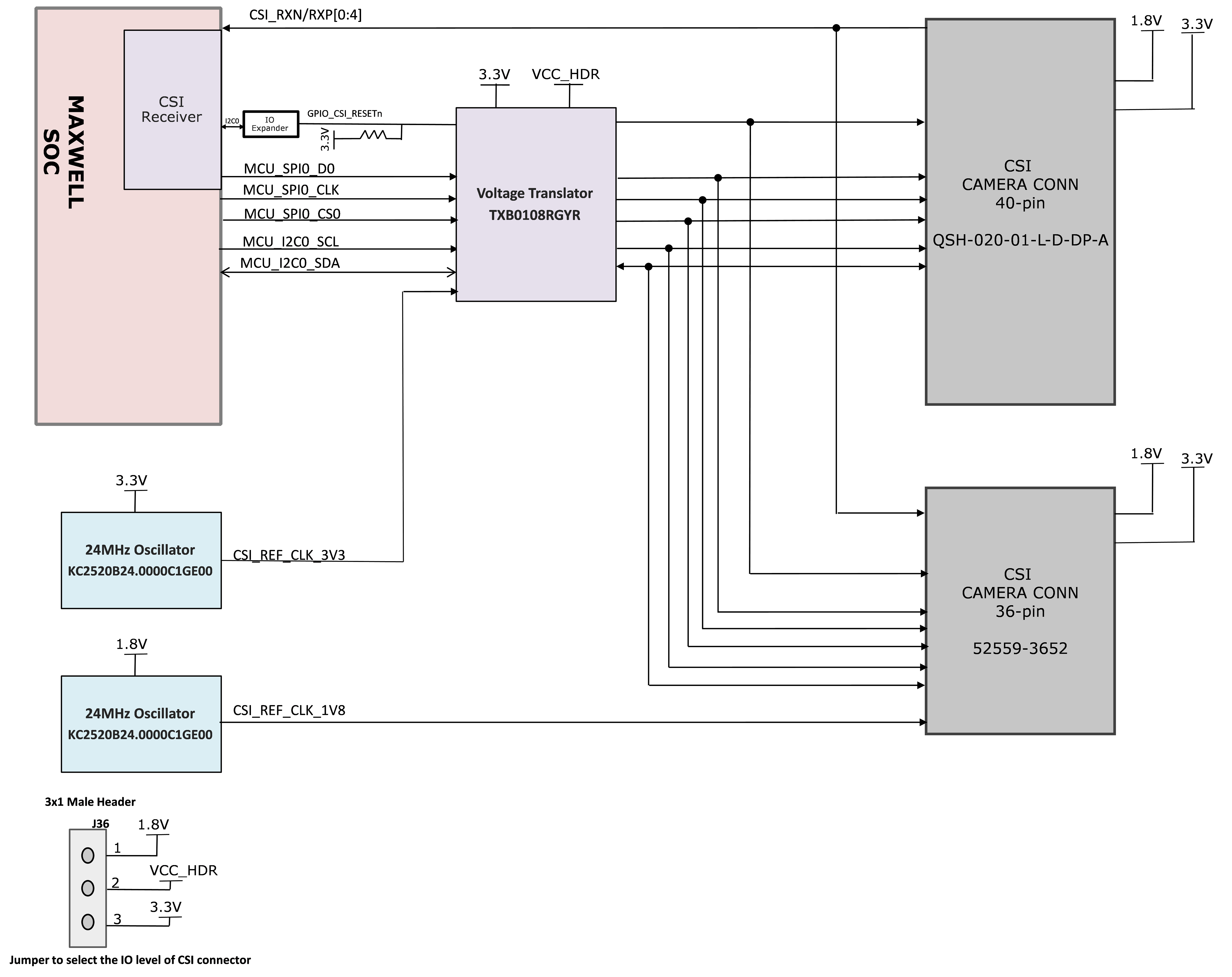
The CSI-2 interface from the AM65x processor is terminated to two camera connectors to interface a CSI-2 standard camera:
- J22 – 40-pin Samtec connector, which is referenced from OV490 / OV10640 Combo Module
- J39 – 36-pin Molex connector, which is referred from Leopard Imaging CPI (VIN) Connector
The two connectors match the existing standards for camera cards. The CSI-2 connector on the board is selected based on the camera module installed. MCU_I2C0 and MCU_SPI0 are also connected to the camera connector through level translators.
The control signals connected to J39 are all 1.8 V, whereas the control signals connected to J22 can be either 1.8 V or 3.3 V. A jumper (J37) is used to select the required I/O voltage, as shown in Figure 3-20. Short Pin 1 and Pin 2 for 1.8-V I/O operation, or Short Pin 2 and Pin 3 for 3.3-V I/O operation. The footprint to mount the oscillator of part number KC2520B24.0000C1GE00 is provided to supply 24-MHz REFCLK to the CSI-2 module. Mount U114 for 1.8-V REFCLK, and mount U112 for 3.3-V REFCLK.
 Figure 3-20 CSI Interface
| Pin Number | CP Card Signals-CSI | Direction |
|---|---|---|
| 1 | NC | NA |
| 2 | CSI_MCU_SCL | Output |
| 3 | NC | NA |
| 4 | CSI_MCU_SDA | Bidirectional |
| 5 | CSI0_RXP0 | Input |
| 6 | NC | NA |
| 7 | CSI0_RXN0 | Input |
| 8 | NC | NA |
| 9 | CSI0_RXP1 | Input |
| 10 | CSI_REF_CLK | Output |
| 11 | CSI0_RXN1 | Input |
| 12 | DGND | Power |
| 13 | CSI0_RXP2 | Input |
| 14 | CSI_RESETN | Output |
| 15 | CSI0_RXN2 | Input |
| 16 | DGND | Power |
| 17 | CSI0_RXP3 | Input |
| 18 | CSI_MCU_SPI0_D0 | Output |
| 19 | CSI0_RXN3 | Input |
| 20 | CSI_MCU_SPI0_CLK | Output |
| 21 | CSI0_RXP4 | Input |
| 22 | CSI_MCU_SPI0_CS0 | Output |
| 23 | CSI0_RXN4 | Input |
| 24 | DGND | Power |
| 25 | NC | NA |
| 26 | NC | NA |
| 27 | NC | NA |
| 28 | NC | NA |
| 29 | NC | NA |
| 30 | VCC3V3_IO | Power |
| 31 | NC | NA |
| 32 | VCC3V3_IO | Power |
| 33 | NC | NA |
| 34 | VCC3V3_IO | Power |
| 35 | NC | NA |
| 36 | VCC3V3_IO | Power |
| 37 | NC | NA |
| 38 | VCC1V8 | Power |
| 39 | NC | NA |
| 40 | VCC1V8 | DGND |
| Pin Number | CP Card Signals-CSI | Direction |
|---|---|---|
| 1 | VCC3V3_IO | Power |
| 2 | VCC3V3_IO | Power |
| 3 | VCC3V3_IO | Power |
| 4 | VCC1V8 | Power |
| 5 | VCC1V8 | Power |
| 6 | DGND | DGND |
| 7 | DGND | NC |
| 8 | CSI0_RXP0 | Input |
| 9 | CSI0_RXN0 | Input |
| 10 | DGND | Power |
| 11 | CSI0_RXP1 | Input |
| 12 | CSI0_RXN1 | Input |
| 13 | DGND | Power |
| 14 | CSI0_RXP2 | Input |
| 15 | CSI0_RXN2 | Input |
| 16 | DGND | Power |
| 17 | CSI0_RXP3 | Input |
| 18 | CSI0_RXN3 | Input |
| 19 | DGND | Power |
| 20 | CSI0_RXP4 | Input |
| 21 | CSI0_RXN4 | Input |
| 22 | DGND | Power |
| 23 | CSI_RESETN | Output |
| 24 | CSI_MCU_SDA | Bidirectional |
| 25 | CSI_MCU_SCL | Output |
| 26 | CSI_REF_CLK_1V8 | Output |
| 27 | NC | NA |
| 28 | NC | NA |
| 29 | DGND | Power |
| 30 | CSI_MCU_SPI0_D0 | Output |
| 31 | CSI_MCU_SPI0_CLK | Output |
| 32 | CSI_MCU_SPI0_CS0 | Output |
| 33 | DGND | Power |
| 34 | DGND | Power |
| 35 | NC | NA |
| 36 | NC | NA |