SPRUIR3B September 2019 – June 2022
6 Hardware References
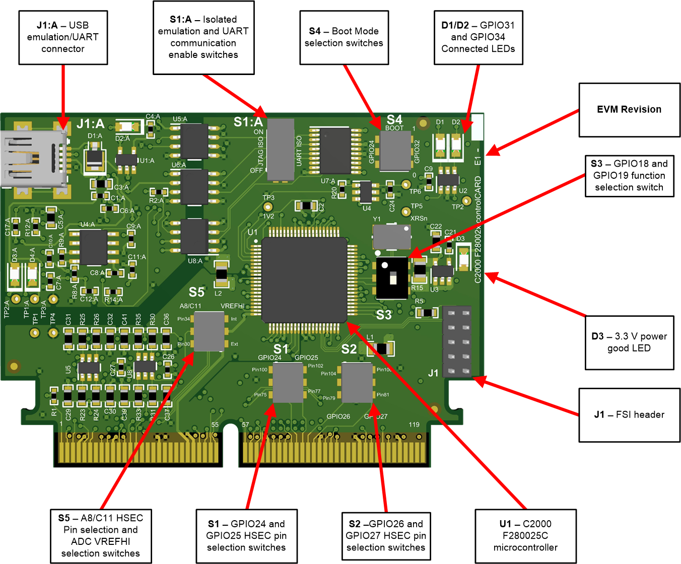
 Figure 6-1 Key Components on the controlCARD - Front
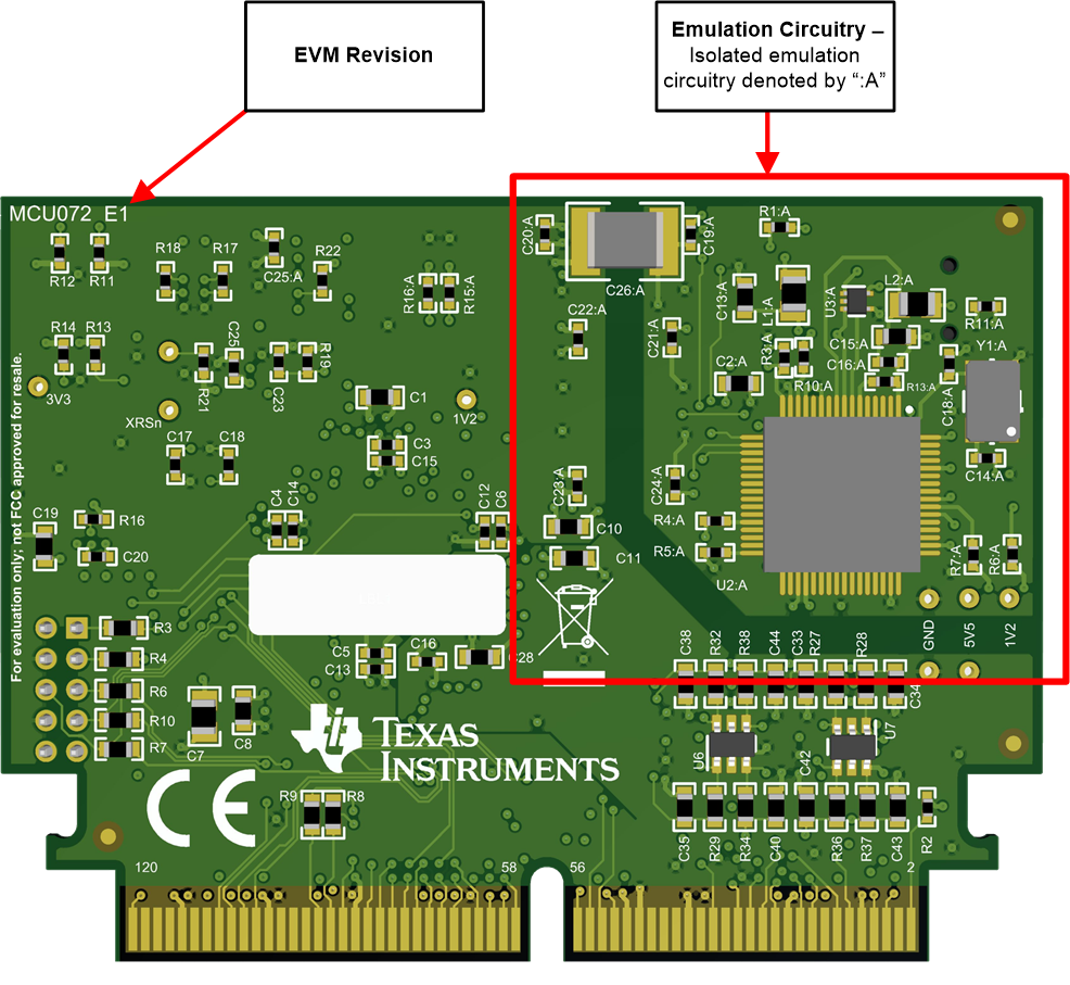
 Figure 6-2 Key Components on the controlCARD - Back
When the controlCARD is used in a high-voltage setup, it is the user’s responsibility to confirm that the voltages and isolation requirements are identified and understood prior to energizing the board or simulation. When energized, the controlCARD or components connected to the controlCARD should not be touched. Furthermore, the capacitor C26:A should be removed to minimize the possibility of leakage current flowing across the isolation barrier of the controlCARD.
| Connectors | |
|---|---|
| J1:A | Emulation/UART connector - USB mini A connector used to provide XDS100v2 emulation and USB-to-UART (SCI) communication through FTDI logic. S1:A determines which connections are enabled to the MCU. |
| J1 | FSI Header – Updated over previous designs. This header is now keyed, contains 2 data lines, and has 3.3 V power. |
| LEDs | |
|---|---|
| D2:A | Turns on when ISO JTAG logic is powered on (green) |
| D3:A | JTAG/UART RX toggle indicator (blue) |
| D4:A | JTAG/UART TX toggle indicator (blue) |
| D1 | Controlled by GPIO–31 with negative logic (red) |
| D2 | Controlled by GPIO–34 with negative logic (red) |
| D3 | Turns on when the controlCARD is powered ON (green) |
| Resistors and Capacitors | |
|---|---|
| R23-R38 | ADC RC input filter resistors: Series resistors which can be used to create an RC filter on the ADC's input. |
| C29-C44 | ADC RC input filter capacitors: Optional capacitors, not populated by default, for the ADC input's RC filters. |
| Switches | |
|---|---|
| S1:A | Isolated emulation and UART communication enable switches: |
S1:A
Position 1 – JTAG Enable:
|
|
|
S1:A Position 2 – ISO UART communication enable:
|
|
| S1 | QEP and SPIB selection switch: This switch allows GPIO24 and GPIO25 to be routed to one of two locations on the HSEC connector. |
| S2 | QEP and SPIB selection switch: This switch allows GPIO26 and GPIO27 to be routed to one of two locations on the HSEC connector. |
| S3 | SPIA or external crystal selection switch: This switch enables the use of SPIA or an external crystal. This methodology was required to support the full range of TI's baseboards and is not recommended in a production system. For full details, see Section 5.2. |
| S4 | Boot Mode Switch: Controls the Boot Options of the F280025C device, see Table 6-2. For a full description, see the device-specific data sheet. |
| S5 | Analog Configuration Switch: |
| S4
Position 1 (left switch) – ADC channel A8/C11 HSEC pin selection
|
|
Position
2 (right switch) - ADC voltage reference selection.
|
|
| Test Points | |
|---|---|
| TP1:A | Emulator 5.0 V input: This power domain is isolated from the other 5.0V domain. |
| TP2:A | Emulator 3.3 V input: This power domain is isolated from the other 3.3 V domains. |
| TP3:A | Emulator ground |
| TP1 | HSEC 5.0 V input: 5.0 V input provided to the 3.3 V voltage regulator to create the unfiltered 3.3 V power. |
| TP2 | Unfiltered 3.3 V: Provides power to the F280025C device. |
| TP3 | MCU 1.2 V: VDD 'core supply' to the F280025C device. Note that this controlCARD has been designed to use the internal voltage regulator. |
| TP4 | Device Ground |
| TP5 | XRSn of F280025C device: Connected to the undervoltage output from the 3.3 V voltage supervisor. |
| TP6 | Overvoltage output: Connected to the overvoltage output from the 3.3 V voltage supervisor. |
On the front of the controlCARD test points are indicated by their TPx number.
On the back of the controlCARD test points are indicated by their signal.
| Mode | Switch Position 1(left switch, GPIO-24) | Switch Position 2 (right switch, GPIO-32) | Boot From |
|---|---|---|---|
| 00 | 0 (down) | 0 (down) | Parallel I/O |
| 01 | 1 (up) | 0 (down) | SCI/Wait Boot |
| 02 | 0 (down) | 1 (up) | CAN |
| 03 | 1 (up) | 1 (up) | Flash/USB |