SPRUIS4E March 2022 – January 2024
- 1
- Jacinto7 J721E/DRA829/TDA4VM Evaluation Module (EVM)
- Trademarks
- 1Introduction
- 2J721E EVM Overview
- 3EVM User Setup/Configuration
-
4J721E EVM Hardware Architecture
- 4.1 J721E EVM Hardware Top level Diagram
- 4.2 J721E EVM Interface Mapping
- 4.3 I2C Address Mapping
- 4.4 GPIO Mapping
- 4.5 Power Supply
- 4.6 Reset
- 4.7 Clock
- 4.8 Memory Interfaces
- 4.9 MCU Ethernet Interface
- 4.10 QSGMII Ethernet Interface
- 4.11 PCIe Interface
- 4.12 USB Interface
- 4.13 CAN Interface
- 4.14 FPD Interface (Audio Deserializer)
- 4.15 FPD Panel Interface (DSI Video Serializer)
- 4.16 Display Serial Interface (DSI) FPC
- 4.17 Audio Interface
- 4.18 Display Port Interface
- 4.19 MLB Interface
- 4.20 I3C Interface
- 4.21 ADC Interface
- 4.22 RTC Interface
- 4.23 Apple Authentication Header
- 4.24 EVM Expansion Connectors
- 4.25 ENET Expansion Connector
- 4.26 CSI Expansion Connector
- 5Revision History
3.6 JTAG Emulation
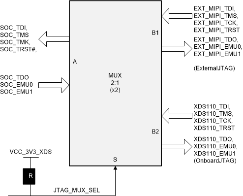
The Common processor board includes XDS110 class on board emulation through the micro B connector J3. It also has an option to support external emulation through MIPI 60 pin header (J16). When an external emulator is connected, XDS110 emulation circuitry path will be disconnected automatically.
 Figure 3-8 JTAG Mux
| Condition | MUX_SEL | Function |
|---|---|---|
| XDS110 Powered via USB | HIGH | A<->B2 port [On Board EMU] |
| External Emulator attached | LOW | A<->B1 port [EXTERNAL EMU] |
As mentioned, the design includes a MIPI 60pin (J16) connector with connections for both JTAG and Trace capabilities. The trace pins are multiplexed with other functions (McASP10, McASP11 and GPMC0) and uses an on-board mux to select the different functions. The mux is defaulted to the MIPI 60pin connector. The 1:3 mux is controlled by bits of the I2C GPIO expander2 (I2C add: 0x22; I2C Inst:I2C0) on the common processor board. There is an option to set the state using the DIP switch SW3 Position 2, which allows GPMC to expansion interface to be selected by default (for boot support).
| Pin No. | Signal | Pin No. | Signal |
|---|---|---|---|
| 1 | VSYS_IO_3V3 | 31 | TRC_DATA6 |
| 2 | MIPI_TMS | 32 | NC |
| 3 | MIPI_TCK | 33 | TRC_DATA7 |
| 4 | MIPI_TDO | 34 | NC |
| 5 | MIPI_TDI | 35 | TRC_DATA8 |
| 6 | MIPI_TGTRST# | 36 | NC |
| 7 | MIPI_RTCK | 37 | TRC_DATA9 |
| 8 | MIPI_TRST_PD (EXT_MIPI_TRST#) |
38 | EXT_MIPI_EMU0 |
| 9 | MIPI_nTRSTPU | 39 | TRC_DATA10 |
| 10 | NC | 40 | EXT_MIPI_EMU1 |
| 11 | NC | 41 | TRC_DATA11 |
| 12 | VSYS_IO_3V3 | 42 | NC |
| 13 | TRC_CLK | 43 | TRC_DATA12 |
| 14 | NC | 44 | NC |
| 15 | DGND | 45 | TRC_DATA13 |
| 16 | DGND | 46 | NC |
| 17 | TRC_CTL | 47 | TRC_DATA14 |
| 18 | TRC_DATA19 | 48 | NC |
| 19 | TRC_DATA0 | 49 | TRC_DATA15 |
| 20 | TRC_DATA20 | 50 | NC |
| 21 | TRC_DATA1 | 51 | TRC_DATA16 |
| 22 | TRC_DATA21 | 52 | NC |
| 23 | TRC_DATA2 | 53 | TRC_DATA17 |
| 24 | NC | 54 | NC |
| 25 | TRC_DATA3 | 55 | TRC_DATA18 |
| 26 | NC | 56 | NC |
| 27 | TRC_DATA4 | 57 | DGND |
| 28 | NC | 58 | JTAG_MUX_SEL |
| 29 | TRC_DATA5 | 59 | NC |
| 30 | NC | 60 | NC |
The EVM Common processor board Kit includes two JTAG converters, one is to convert MIPI 60 pin to TI14 pin JTAG emulator and the other one is to convert MIPI 60 pin to CTI20 pin JTAG.
Table 3-13 shows pinouts of the TI14 pin and the CTI 20 pin JTAG converters.
| Pin No. | Signal | Pin No. | Signal |
|---|---|---|---|
| 1 | MIPI_20_TMS | 11 | MIPI_20_TCK |
| 2 | MIPI_20_TRST | 12 | DGND |
| 3 | MIPI_20_TDI | 13 | MIPI_20_EMU0 |
| 4 | MIPI_20_TDIS | 14 | MIPI_20_EMU1 |
| 5 | MIPI_20_VTREF | 15 | SYSRST# |
| 6 | NC (key) | 16 | DGND |
| 7 | MIPI_20_TDO | 17 | NC |
| 8 | 20PJTAG_DET | 18 | NC |
| 9 | MIPI_20_RTCK | 19 | NC |
| 10 | DGND | 20 | DGND |
| Pin No. | Signal | Pin No. | Signal |
|---|---|---|---|
| 1 | MIPI_14_TMS | 8 | 14PJTAG_DET |
| 2 | MIPI_14_TRST | 9 | MIPI_14_RTCK |
| 3 | MIPI_14_TDI | 10 | DGND |
| 4 | MIPI_14_TDIS | 11 | MIPI_14_TCK |
| 5 | MIPI_14_VTREF | 12 | DGND |
| 6 | NC (key) | 13 | MIPI_14_EMU0 |
| 7 | MIPI_14_TDO | 14 | MIPI_14_EMU1 |