SPRUIS4E March   2022  – January 2024


  1.   1
  2.   Jacinto7 J721E/DRA829/TDA4VM Evaluation Module (EVM)
  3.   Trademarks
  4. 1Introduction
    1. 1.1 Key Features
    2. 1.2 Thermal Compliance
    3. 1.3 REACH Compliance
    4. 1.4 EMC, EMI, and ESD Compliance
  5. 2J721E EVM Overview
    1. 2.1 J721E EVM Board Identification
    2. 2.2 J721E SOM Component Identification
    3. 2.3 Jacinto7 Common Processor Components Identification
    4. 2.4 Quad Ethernet Components Identification
  6. 3EVM User Setup/Configuration
    1. 3.1 Power Requirements
    2. 3.2 Power ON Switch and Power LEDs
      1. 3.2.1 Over Voltage and Under Voltage Protection Circuit
      2. 3.2.2 Power Regulators and Power Status LEDs
    3. 3.3 EVM Reset/Interrupt Push Buttons
    4. 3.4 EVM DIP Switches
      1. 3.4.1 EVM Configuration DIP Switch
      2. 3.4.2 SOM Configuration DIP Switch
      3. 3.4.3 Boot Modes
      4. 3.4.4 Other Selection Switches
    5. 3.5 EVM UART/COM Port Mapping
    6. 3.6 JTAG Emulation
  7. 4J721E EVM Hardware Architecture
    1. 4.1  J721E EVM Hardware Top level Diagram
    2. 4.2  J721E EVM Interface Mapping
    3. 4.3  I2C Address Mapping
    4. 4.4  GPIO Mapping
    5. 4.5  Power Supply
      1. 4.5.1 Power Sequencing
      2. 4.5.2 Voltage Supervisor
      3. 4.5.3 DDR I/O Voltage Selection
        1. 4.5.3.1 J721E SoC S2R Logic Flow Diagram
        2. 4.5.3.2 J721E SoC MCU Only Operation
        3. 4.5.3.3 Power Monitoring
    6. 4.6  Reset
    7. 4.7  Clock
      1. 4.7.1 Processor’s Primary Clock
      2. 4.7.2 Processor’s Secondary/SERDES Ref Clock
      3. 4.7.3 EVM Peripheral Ref Clock
    8. 4.8  Memory Interfaces
      1. 4.8.1 LPDDR4 Interface
      2. 4.8.2 OSPI Interface
      3. 4.8.3 UFS Interface
      4. 4.8.4 MMC Interface
        1. 4.8.4.1 MMC0 - eMMC Interface
        2. 4.8.4.2 MMC1 – Micro SD Interface
      5. 4.8.5 Board ID EEPROM Interface
      6. 4.8.6 Boot EEPROM Interface
    9. 4.9  MCU Ethernet Interface
      1. 4.9.1 Gigabit Ethernet PHY Default Configuration
    10. 4.10 QSGMII Ethernet Interface
    11. 4.11 PCIe Interface
      1. 4.11.1 X1 Lane PCIe Interface
      2. 4.11.2 X2 Lane PCIe Interface
      3. 4.11.3 M.2 PCIe Interface
    12. 4.12 USB Interface
      1. 4.12.1 USB 3.1 Interface
      2. 4.12.2 USB 2.0 Interface
      3. 4.12.3 USB 3.0 Micro AB Interface (Reserved Port)
    13. 4.13 CAN Interface
    14. 4.14 FPD Interface (Audio Deserializer)
    15. 4.15 FPD Panel Interface (DSI Video Serializer)
    16. 4.16 Display Serial Interface (DSI) FPC
    17. 4.17 Audio Interface
    18. 4.18 Display Port Interface
    19. 4.19 MLB Interface
    20. 4.20 I3C Interface
    21. 4.21 ADC Interface
    22. 4.22 RTC Interface
    23. 4.23 Apple Authentication Header
    24. 4.24 EVM Expansion Connectors
    25. 4.25 ENET Expansion Connector
      1. 4.25.1 Power Requirements
      2. 4.25.2 Clock
        1. 4.25.2.1 Main Clock
        2. 4.25.2.2 Optional Clock
      3. 4.25.3 Reset Signals
      4. 4.25.4 Ethernet Interface
        1. 4.25.4.1 Quad Port SGMII PHY Default Configuration
      5. 4.25.5 Board ID EEPROM Interface
    26. 4.26 CSI Expansion Connector
  8. 5Revision History

Power Requirements

This EVM supports a wide input range of 6 V to 28 V. There is a DC Jack provided for supplying the input power (J7). An external power supply is required to power the EVM but is not included as part of the EVM kit. The external power supply requirements are:

  • Power Jack: 2.5 mm ID, 5.5 mm OD
  • Nom Voltage: 12 VDC, Recommended Minimum Current: 5000 mA
Table 3-1 Recommended External Power Supply
DigiKey Part No Manufacturer Manufacturer Part No
SDI65-12-U-P6-ND CUI Inc. SDI65-12-U-P6
SDI65-12-UD-P6-ND CUI Inc. SDI65-12-UD-P6

EVM’s 2.5 x 5.5-mm DC barrel jack connector (J7) supports 10-A current rating. Polarity outside barrel is Negative/GND, inside post is Positive/PWR.
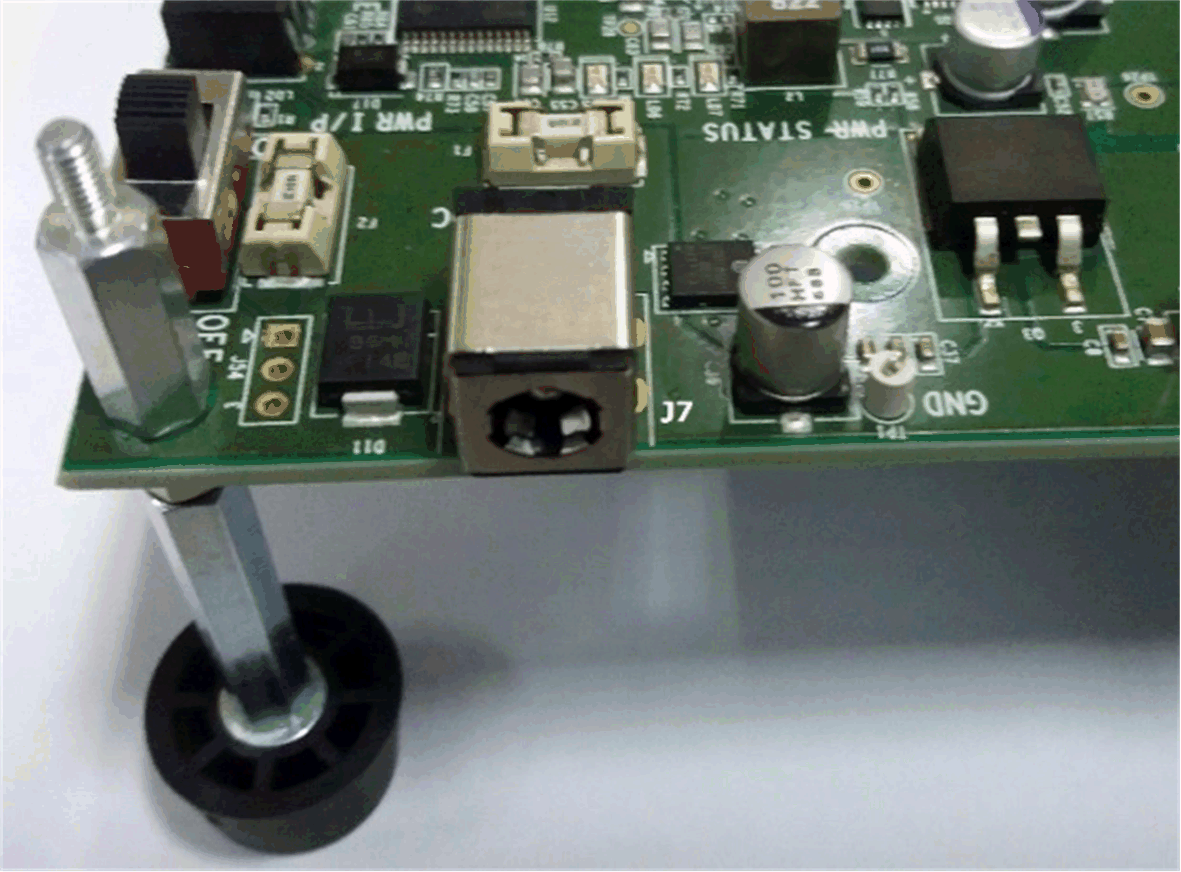
GUID-DA86557E-9756-4EEC-9396-DF65F71BA6E5-low.gif Figure 3-1 Connector Used for Power Input