SPRUIT1B May   2020  – November 2020


  1.   Trademarks
  2. 1Introduction
    1. 1.1 Key Features
  3. 2GESI Expansion Board Overview
    1. 2.1 GESI Expansion Board Identification
    2. 2.2 GESI Expansion Board Component Identification
  4. 3GESI Expansion Board - User Setup/Configuration
    1. 3.1 GESI Infotainment Expansion Board With CP Board
      1. 3.1.1 Board Assembly Procedures
    2. 3.2 Power Requirements
    3. 3.3 EVM Reset/Interrupt Push Buttons
    4. 3.4 EVM Configuration DIP Switch
  5. 4GESI Expansion Board Hardware Architecture
    1. 4.1  GESI Expansion Board Hardware Top Level Diagram
    2. 4.2  Expansion Connectors
    3. 4.3  Board ID EEPROM
    4. 4.4  Ethernet Interface
      1. 4.4.1 RGMII Clocking Scheme
      2. 4.4.2 Ethernet Port LED Indication
    5. 4.5  PROFI BUS / RS485
    6. 4.6  LIN Interface
    7. 4.7  MCAN
    8. 4.8  MUX Selection
      1. 4.8.1 MUX – PRGx_MDIO/MDC, CPSW9G_MDIO/MDC
      2. 4.8.2 MUX – PRG1_RGMII1/PRG1_PWM
      3. 4.8.3 MUX – PRG1_PWM/MCAN
      4. 4.8.4 MUX_MC/BP_SEL
    9. 4.9  GESI LaunchPad-Booster Pack Interface
    10. 4.10 Motor Control Interface
    11. 4.11 USS/IMU Header
    12. 4.12 Test Header
  6.   A Interface Mapping
  7.   B GESI Board GPIO Mapping
  8.   C I2C Address Mapping
  9.   D Revision History

MUX – PRG1_RGMII1/PRG1_PWM

PRG1_RGMII1 and PWM signals of J721E SoC is interfaced on the GESI Expansion board using Resistor Mux as shown in Figure 4-10. J721E signals go to either Ethernet PHY or Motor Control interface on the GESI expansion board. The default path is provided to Ethernet.

Users are required to change the Resistor population option when they need to interface with Motor Control Interface (PWM).
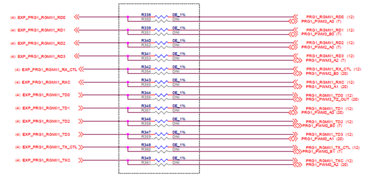
GUID-43E5DA94-6031-48E8-BD41-ACFD34D1CE9A-low.png Figure 4-10 Resistor MUX for EXP_PRG1_RGMII1 Signal