SPRUIW7A October 2020 – February 2022
- Trademarks
- 1Introduction
- 2J7200 EVM Overview
- 3EVM User Setup/Configuration
-
4J7200 EVM Hardware Architecture
- 4.1 J7200 EVM Hardware Top Level Diagram
- 4.2 J7200 EVM Interface Mapping
- 4.3 I2C Address Mapping
- 4.4 GPIO Mapping
- 4.5 Power Supply
- 4.6 Reset
- 4.7 Clock
- 4.8 Memory Interfaces
- 4.9 MCU Ethernet Interface
- 4.10 QSGMII Ethernet Interface
- 4.11 PCIe Interface
- 4.12 USB Interface
- 4.13 Audio Interface
- 4.14 CAN Interface
- 4.15 FPD Interface (Audio Deserializer)
- 4.16 I3C Interface
- 4.17 ADC Interface
- 4.18 RTC Interface
- 4.19 Apple Authentication Header
- 4.20 JTAG Emulation
- 4.21 EVM Expansion Connectors
- 4.22 ENET Expansion Connector
- 5Functional Safety
- 6Revision History
4.10 QSGMII Ethernet Interface
The SERDES0 SGMII1 signals of J7200 SoC is interfaced to Quad SGMII PHY VSC8514XMK-11 on the Quad Port Ethernet board through CP board, two stacked RJ45 connectors with integrated magnetics PN# LPJG17512AONL used for external communication.
The VC8514 device includes three external PHY address pins, PHYADD [4:2] to allow control of multiple PHY devices on a system board sharing a common management bus. These pins set the most significant bits of the PHY address port map. The lower two bits of the address for each port are derived from the physical address of the port (0 to 3) and the setting of the PHY address reversal bit in register 20E1, bit 9.
Reference clock 156.25 MHz to the PHY is generated from SERDES clock generator (CDCI2) on the CP board by default. Optionally, clock generator on the Quad Port Ethernet board also can provide the clock to the PHY with resistor option.
| Clock Source | Install | Remove |
|---|---|---|
| From CP Board (Default) | R1, R2 | R3, R4 |
| From On board clock generator | R3, R4 | R1, R2 |
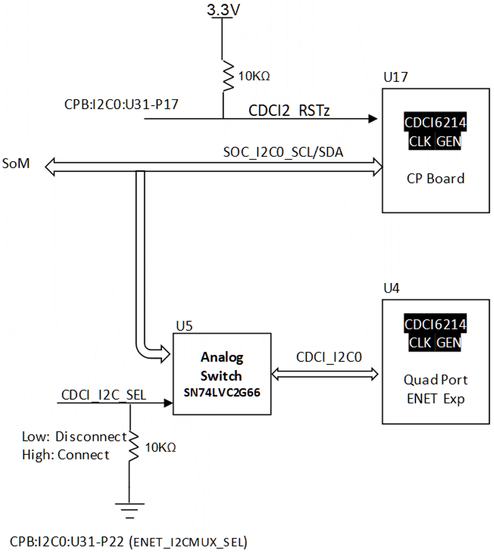
If using the alternate clock source for reference, the programming of the clock generate is done through I2C0 port of the SoC. I2C signals to the on board clock generator is connected through an active switch and paths are disconnected by pulling the CDCI_I2C_SEL signal low. Since, both on board and CP board clock generator has same I2C slave address, programming of these clock generator needs special attention. While programming on board clock generator, the clock generator (CDCI2) on the common processor boards needs to be under reset.
 Figure 4-18 Quad-SGMII Board I2C
Coupling capacitors (0.1 μF) added in series at the respective driver ends on the QSGMII data signals.
Below are the address and clock configurations:
PHY0: 10000 0X10
PHY1: 10001 0X11
PHY2: 10010 0X12
PHY3: 10011 0X13
The resistor strapping options are shown in Figure 4-19.
 Figure 4-19 QSGMII Ethernet PHY
Settings