SPRUIW8 November   2020


  1.   Trademarks
  2. 1Board Overview
    1. 1.1 Kit Contents
    2. 1.2 Features
    3. 1.3 Specifications
    4. 1.4 Using the F28002x LaunchPad
    5. 1.5 BoosterPacks
    6. 1.6 Hardware Revisions
      1. 1.6.1 Revision A
  3. 2Software Development
    1. 2.1 Software Tools and Packages
    2. 2.2 F28002x LaunchPad Demo Program
    3. 2.3 Programming and Running Other Software on the F28002x LaunchPad
  4. 3Hardware Description
    1. 3.1 Functional Description and Connections
      1. 3.1.1  Microcontroller
      2. 3.1.2  LEDs
      3. 3.1.3  Encoder Connectors
      4. 3.1.4  FSI
      5. 3.1.5  CAN
      6. 3.1.6  CLB
      7. 3.1.7  Boot Modes
      8. 3.1.8  BoosterPack Headers
        1. 3.1.8.1 BoosterPack Sites
      9. 3.1.9  Analog Voltage Reference Header
      10. 3.1.10 Other Headers and Jumpers
        1. 3.1.10.1 USB Isolation Block
        2. 3.1.10.2 BoosterPack Site 2 Power Isolation
        3. 3.1.10.3 Alternate Power
        4. 3.1.10.4 5 V Step-up Converter
    2. 3.2 Debug Interface
      1. 3.2.1 XDS110 Debug Probe
      2. 3.2.2 XDS110 Output
      3. 3.2.3 Virtual COM Port
    3. 3.3 Alternate Routing
      1. 3.3.1 Overview
      2. 3.3.2 UART Routing
      3. 3.3.3 EQEP Routing
      4. 3.3.4 CAN Routing
      5. 3.3.5 FSI Routing
      6. 3.3.6 X1/X2 Routing
      7. 3.3.7 PWM DAC
      8. 3.3.8 Other GPIOs
  5. 4Board Design
    1. 4.1 Schematic
    2. 4.2 PCB Layout
    3. 4.3 BOM
    4. 4.4 LAUNCHXL-F280025C Board Dimensions
  6. 5Frequently Asked Questions
  7. 6References
    1. 6.1 Reference Documents
    2. 6.2 Other TI Components Used in This Design

F28002x LaunchPad Demo Program

The LAUNCHXL-F280025C includes a TMSF280025CPNS device pre-programmed with a demo program. When the LaunchPad is powered on the demo program begins with an LED blink sequence on LED4 and LED5. After a few seconds the device switches into an ADC sampling mode.

Every 1 second the ADC samples pin ADCINA6 and the sampled value is represented as follows: If the sample is above mid-scale (2048), the red LED4 will illuminate. If the sample is below mid-scale, the green LED5 will illuminate.

In addition to the LED indicators, ADC sample results are also displayed on your PC through the USB/UART connection. To view the UART information on your PC, first determine the COM port associated with the LaunchPad. To do this in Windows open the Device Manager. Look for an entry under Ports (COM & LPT) titled "XDS110 Class Application/User UART (COMX)", where X is a number. Remember this number for when you open a serial terminal.

GUID-20201008-CA0I-LSJX-8FH0-MLQ9FGGPTHXV-low.pngFigure 2-1 LaunchPad XDS110 COM Port
The demo application's UART data was tested using PuTTY, which is a free and open-source terminal emulator. To view the UART data in a serial terminal program open the COM port found using the Windows Device Manager with the following settings.

115200 Baud, 8 data bits, no parity, 1 stop bit.

After properly opening the serial port in your serial terminal, reset the LaunchPad by pressing the S1 reset button and observe the serial terminal to see the TI logo in ASCII art.
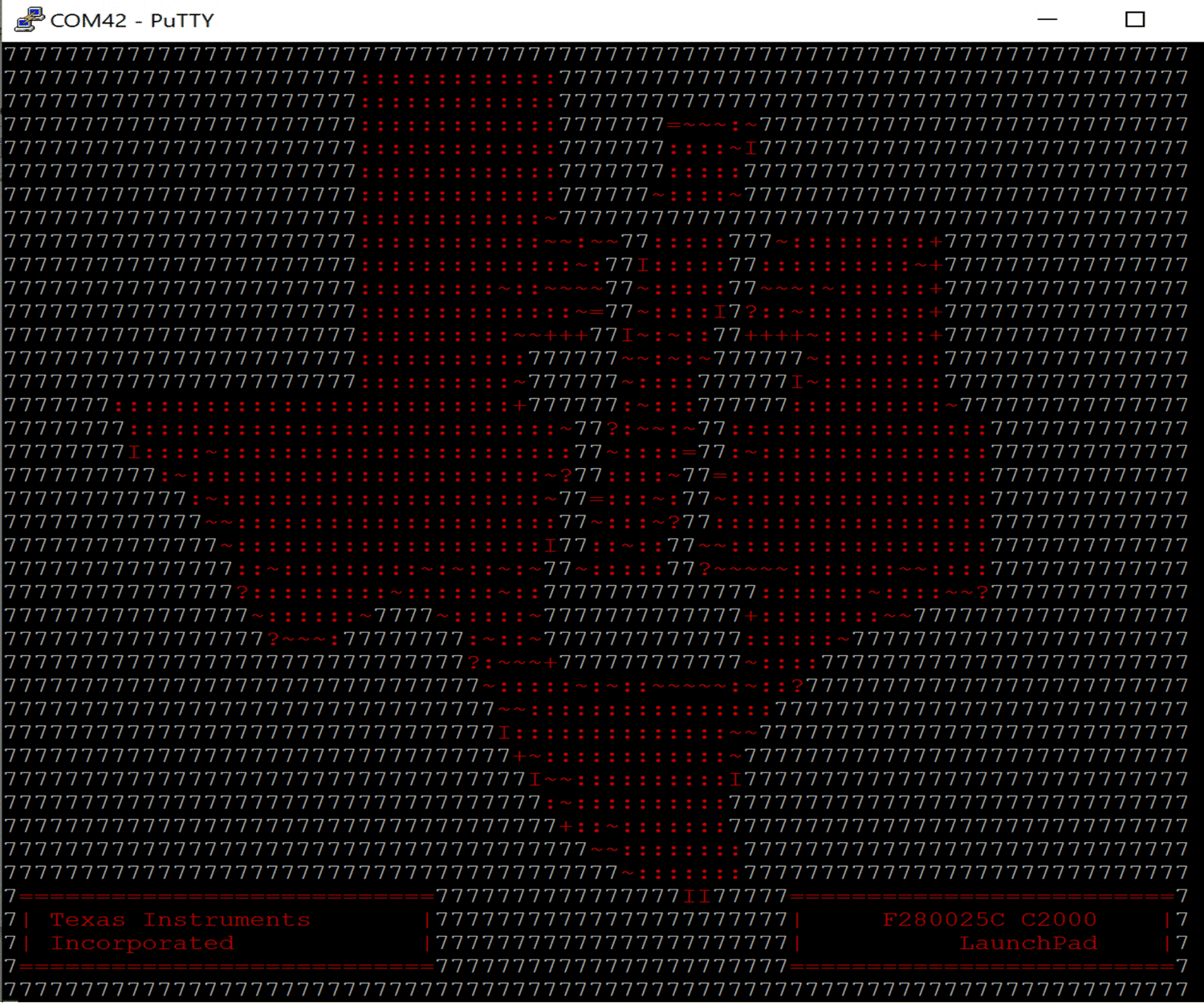
GUID-20201008-CA0I-BNTZ-62JZ-HZBCDFS4DN6H-low.pngFigure 2-2 LaunchPad Demo Serial Terminal - TI Logo
After a few moments the ADC value sampled on the ADCINA6 pin will appear in the bottom right corner of the terminal and be updated each second. Jumper the ADCINA6 header to a 3.3V, GND, or other 0-3.3V signal header to see the on-screen value change.

GUID-20201008-CA0I-HWLC-MJ0N-Q1KBX1B6TD65-low.pngFigure 2-3 LaunchPad Demo Serial Terminal - ADC Sampling