SPRUIW8 November   2020


  1.   Trademarks
  2. 1Board Overview
    1. 1.1 Kit Contents
    2. 1.2 Features
    3. 1.3 Specifications
    4. 1.4 Using the F28002x LaunchPad
    5. 1.5 BoosterPacks
    6. 1.6 Hardware Revisions
      1. 1.6.1 Revision A
  3. 2Software Development
    1. 2.1 Software Tools and Packages
    2. 2.2 F28002x LaunchPad Demo Program
    3. 2.3 Programming and Running Other Software on the F28002x LaunchPad
  4. 3Hardware Description
    1. 3.1 Functional Description and Connections
      1. 3.1.1  Microcontroller
      2. 3.1.2  LEDs
      3. 3.1.3  Encoder Connectors
      4. 3.1.4  FSI
      5. 3.1.5  CAN
      6. 3.1.6  CLB
      7. 3.1.7  Boot Modes
      8. 3.1.8  BoosterPack Headers
        1. 3.1.8.1 BoosterPack Sites
      9. 3.1.9  Analog Voltage Reference Header
      10. 3.1.10 Other Headers and Jumpers
        1. 3.1.10.1 USB Isolation Block
        2. 3.1.10.2 BoosterPack Site 2 Power Isolation
        3. 3.1.10.3 Alternate Power
        4. 3.1.10.4 5 V Step-up Converter
    2. 3.2 Debug Interface
      1. 3.2.1 XDS110 Debug Probe
      2. 3.2.2 XDS110 Output
      3. 3.2.3 Virtual COM Port
    3. 3.3 Alternate Routing
      1. 3.3.1 Overview
      2. 3.3.2 UART Routing
      3. 3.3.3 EQEP Routing
      4. 3.3.4 CAN Routing
      5. 3.3.5 FSI Routing
      6. 3.3.6 X1/X2 Routing
      7. 3.3.7 PWM DAC
      8. 3.3.8 Other GPIOs
  5. 4Board Design
    1. 4.1 Schematic
    2. 4.2 PCB Layout
    3. 4.3 BOM
    4. 4.4 LAUNCHXL-F280025C Board Dimensions
  6. 5Frequently Asked Questions
  7. 6References
    1. 6.1 Reference Documents
    2. 6.2 Other TI Components Used in This Design

LAUNCHXL-F280025C Board Dimensions

Figure 4-10 is a dimensional drawing of the F28002x LaunchPad that shows the location of selected features of the board as well as the component locations.
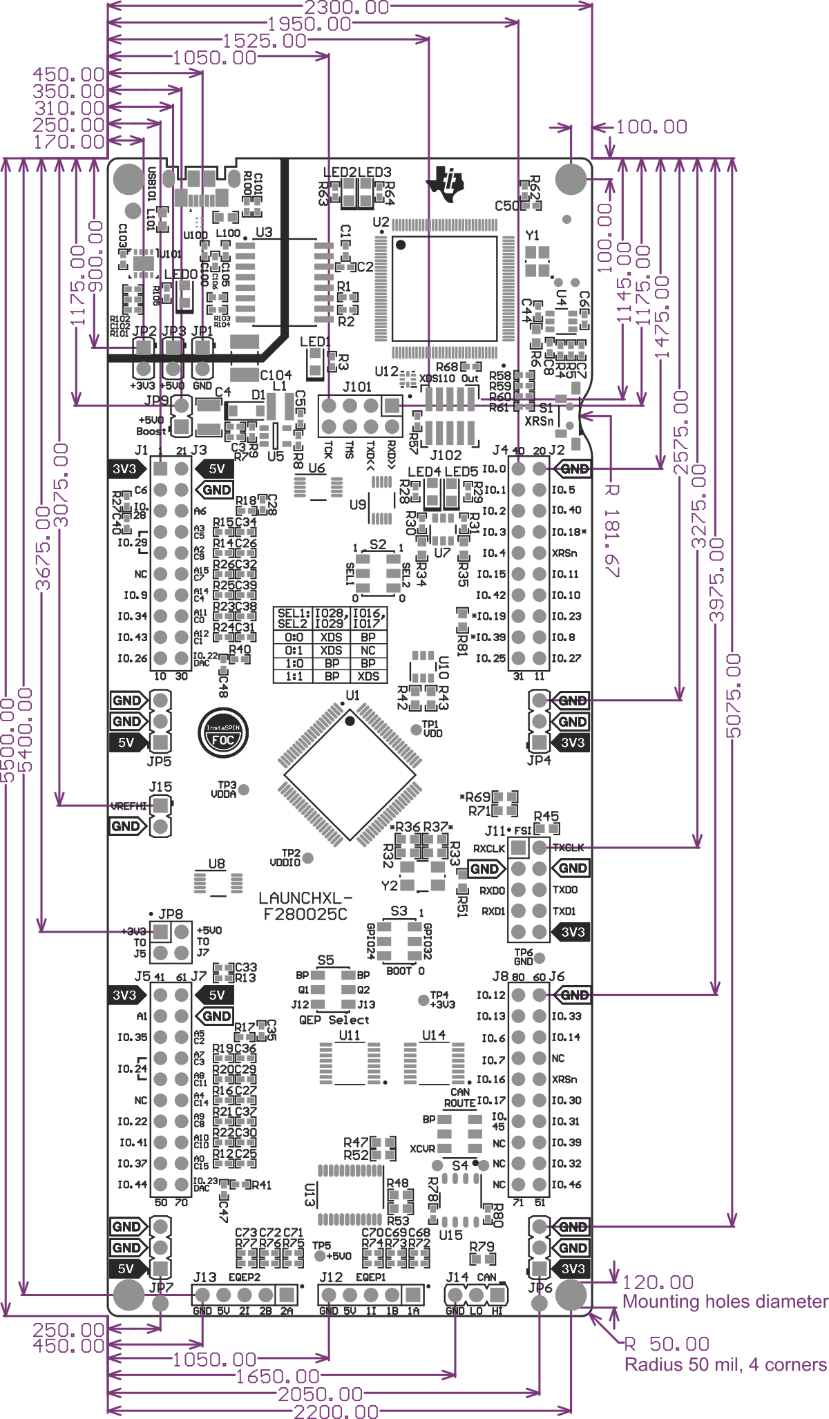
GUID-20201002-CA0I-NH0M-C6CW-FPVBWWDFKK3C-low.pngFigure 4-10 F28002x LaunchPad Dimensions and Component Locations