SPRUIY9B May 2021 – October 2023
- 1
- Abstract
- Trademarks
- 1Key Features
- 2EVM Revisions and Assembly Variants
- 3Important Usage Notes
-
4System Description
- 4.1 Key Features
- 4.2 Functional Block Diagram
- 4.3 Power-On/Off Procedures
- 4.4
Peripheral and Major Component
Description
- 4.4.1 Clocking
- 4.4.2 Reset
- 4.4.3 Power
- 4.4.4 Configuration
- 4.4.5 JTAG
- 4.4.6 Test Automation
- 4.4.7 UART Interface
- 4.4.8 Memory Interfaces
- 4.4.9 Ethernet Interface
- 4.4.10 USB 3.0 Interface
- 4.4.11 PRU Connector
- 4.4.12 User Expansion Connector
- 4.4.13 MCU Connector
- 4.4.14 Interrupt
- 4.4.15 I2C Interface
- 4.4.16 IO Expander (GPIOs)
-
5Known Issues
- 5.1 Issue 1: LP8733x Max output Capacitance Spec Exceeded on LDO0 and LDO1
- 5.2 Issue 2: LP8733x Output Voltage of 0.9V Exceeds AM64x VDDR_CORE max Voltage Spec of 0.895 V
- 5.3 Issue 3 - SDIO Devices on MMC0 Require Careful Trace Lengths to Meet Interface Timing Requirements
- 5.4 Issue 4 - LPDDR4 Data Rate Limitation in Stressful Conditions
- 5.5 Issue 5 - Junk Character
- 5.6 Issue 6 - Test Power Down Signal Floating
- 5.7 Issue 7 - uSD Boot Not Working
- 6Regulatory Compliance
- 7Revision History
4.4.9.2 DP83867 – Power, Clock, Reset, Interrupt and LEDs
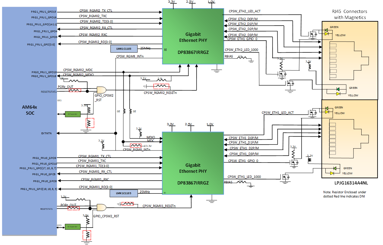
The PHY devices include Integrated MDI Termination Resistors. So external termination is not provided.
Power: The RGMII signals from PRG0 and PRG1 domain is at 3.3V IO level. The Gigabit PHY device DP83867 requires I/O power of 3.3V and analog supply of 2.5V and 1.0V
Clock: A 25 MHz LVCMOS clock is given to the PHYs through clock buffer LMK1C1103 (individual outputs).
Reset: The reset for PHYs is from a circuit that ANDs the PORz_OUT and GPIO from IO expander and an optional RESETSTATz from SoC. By default RESETSTATz is not used for resetting the PHY. The IO expander is controlled through I2C1 port of AM64x SOC. Footprints for both a pull-up and a pull-down resistor are provided to the GPIO to set the default value. Each of the Ethernet PHY’s have separate Reset Signals driven by GPIO’s. A hardware reset is accomplished by applying a low pulse, with a duration of at least 1 micro-second to the RESET_N pin.
Interrupt: The interrupt from two CPSW RGMII PHYs from PRG1 domain are tied together and is connected to EXTINTN pin of AM64x SOC.
Four configurable LED pins and two GPIO of Ethernet PHY are used to indicate link status. Several functions can be multiplexed onto the LEDs for different modes of operation. The LED operation mode can be selected using the LEDCR1 register address 0x0018 on the DP83867 device. The default configurations are as follows.
LED0: By default, this pin indicates that link is established. Additional functionality is configurable via LEDCR1 [3:0] register bits in the DP83867 device. LDE0 is not used in the CPSW PHY (DP83867), this is also a strap pin which is used to set mirror enable. Since these features are not required the strapping for the LED0 is not provided.
LED_1: By default, this pin indicates that 1000BASE-T link is established. This setting can be changed to Auto negotiate to 10/100Mbps using the strap resistors. Additional functionality is configurable via LEDCR1 [7:4] register bits in the DP83867 device. LED_1 is a also an strap pin, which is having internal pull-down resistor to set RGMII TX Clock Skew in the DP83867 device. Since this pin is set to active on both the devices, this results in dim LED lighting when LED is driven directly. So a MOSFET is used to drive LED.
LED_2: By default, this pin indicates receive or transmit activity. Additional functionality is configurable via LEDCR1 [11:18] register bits in the DP83867 device. LED_2 is also a strap pin, which is having internal pull-down resistor to set RGMII TX Clock Skew in the DP83867 device. The default condition is to auto negotiate and advertise link as 10/100/1000Mbps, this can be changed using the strap resistors provided. The pull up resistor used for strap setting results in dim LED lighting when LED is driven directly. So a MOSFET is used to drive LED.
GPIO0: In the DP83867 PHY, the GPIO can be configured to function as LED3 through GPIO Mux Control Register 1 (GPIO_MUX_CTRL1) and the LED configuration can be set by programming LEDCR1 register and this pin is used to indicate operating as a 100-Mbps connection. A MOSFET is used to drive LED as shown in the below figure.
GPIO1: In the DP83867 PHY, the GPIO can be configured to function as LED3 through GPIO Mux Control Register 1 (GPIO_MUX_CTRL1) and the LED configuration can be set by programming LEDCR1 register this is also a strap pin which is used to set fast link drop (FDP), currently this is disabled.
LED Indication in Ethernet RJ45 Connector: LED Control is achieved through an external MOSFET.
RJ45 Connector LED Indication - CPSW (DP83867): LED1 is connected to RJ45 LED (Green) to indicate 1000 MHz link and LED2 is connected to RJ45 LED (Yellow) to indicate transmit/receive activity. LED Control is achieved through an external MOSFET.
 Figure 4-21 Ethernet Interface
Resistors which are highlighted by red color box are DNI components