SPRUIY9B May 2021 – October 2023
- 1
- Abstract
- Trademarks
- 1Key Features
- 2EVM Revisions and Assembly Variants
- 3Important Usage Notes
-
4System Description
- 4.1 Key Features
- 4.2 Functional Block Diagram
- 4.3 Power-On/Off Procedures
- 4.4
Peripheral and Major Component
Description
- 4.4.1 Clocking
- 4.4.2 Reset
- 4.4.3 Power
- 4.4.4 Configuration
- 4.4.5 JTAG
- 4.4.6 Test Automation
- 4.4.7 UART Interface
- 4.4.8 Memory Interfaces
- 4.4.9 Ethernet Interface
- 4.4.10 USB 3.0 Interface
- 4.4.11 PRU Connector
- 4.4.12 User Expansion Connector
- 4.4.13 MCU Connector
- 4.4.14 Interrupt
- 4.4.15 I2C Interface
- 4.4.16 IO Expander (GPIOs)
-
5Known Issues
- 5.1 Issue 1: LP8733x Max output Capacitance Spec Exceeded on LDO0 and LDO1
- 5.2 Issue 2: LP8733x Output Voltage of 0.9V Exceeds AM64x VDDR_CORE max Voltage Spec of 0.895 V
- 5.3 Issue 3 - SDIO Devices on MMC0 Require Careful Trace Lengths to Meet Interface Timing Requirements
- 5.4 Issue 4 - LPDDR4 Data Rate Limitation in Stressful Conditions
- 5.5 Issue 5 - Junk Character
- 5.6 Issue 6 - Test Power Down Signal Floating
- 5.7 Issue 7 - uSD Boot Not Working
- 6Regulatory Compliance
- 7Revision History
4.4.11 PRU Connector
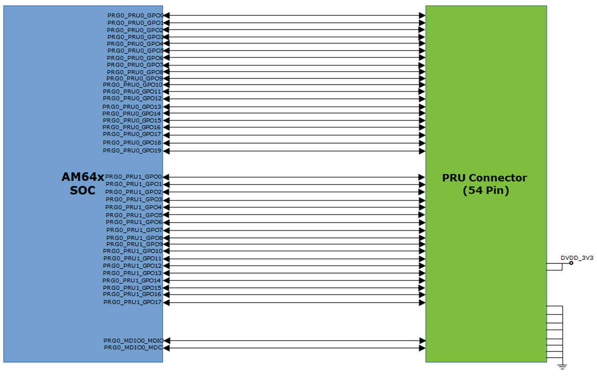
PRU Header offers Low speed connection to PRG0 Interface. PRU_ICSSG signals from PRG0 Port (PRG0_PRU0 and PRG0_PRU1) are terminated on the PRU Expansion Connector. PRU0 signals are connected to a 27x2 standard 0.1” spaced 54 pin connector. Connector shall contain MDIO Control Signals (2 Pins), PRG0_PRU0_GPO [0: 19], PRG0_PRU1_GPO [0: 17], +3.3V PWR (2 Pins) and Ground reference (5 Pins), DETECT, RESET, INT going to the daughter card and SoC I2C0 lines (2 Pins). 3.3V are current limited to 500 mA. This is achieved by using load switch TPS22902YFPR. Enable for the load switch is controlled by SoC.
Signals routed from the PRU Connector are listed in Table 4-20.
| Pin | Net Name | Pin | Net Name |
|---|---|---|---|
| 1 | VCC3V3_PRU | 2 | DGND |
| 3 | PRU_DETECT | 4 | PRU_RESETz |
| 5 | PRU_INTn | 6 | SoC_I2C0_SCL |
| 7 | PRG0_PRU0GPO16 | 8 | SoC_I2C0_SDA |
| 9 | PRG0_MDIO0_MDC | 10 | NC |
| 11 | PRG0_MDIO0_MDIO | 12 | NC |
| 13 | PRG0_PRU0GPO0 | 14 | PRG0_PRU0GPO1 |
| 15 | PRG0_PRU0GPO2 | 16 | PRG0_PRU0GPO3 |
| 17 | PRG0_PRU0GPO4 | 18 | PRG0_PRU0GPO5 |
| 19 | PRG0_PRU0GPO6 | 20 | PRG0_PRU0GPO7 |
| 21 | PRG0_PRU0GPO8 | 22 | PRG0_PRU0GPO9 |
| 23 | PRG0_PRU0GPO10 | 24 | PRG0_PRU0GPO11 |
| 25 | PRG0_PRU0GPO12 | 26 | PRG0_PRU0GPO13 |
| 27 | PRG0_PRU0GPO14 | 28 | PRG0_PRU0GPO15 |
| 29 | DGND | 30 | PRG0_PRU0GPO17 |
| 31 | PRG0_PRU0GPO18 | 32 | PRG0_PRU0GPO19 |
| 33 | DGND | 34 | DGND |
| 35 | PRG0_PRU1GPO0 | 36 | PRG0_PRU1GPO1 |
| 37 | PRG0_PRU1GPO2 | 38 | PRG0_PRU1GPO3 |
| 39 | PRG0_PRU1GPO4 | 40 | PRG0_PRU1GPO5 |
| 41 | PRG0_PRU1GPO6 | 42 | PRG0_PRU1GPO7 |
| 43 | PRG0_PRU1GPO8 | 44 | PRG0_PRU1GPO9 |
| 45 | PRG0_PRU1GPO10 | 46 | PRG0_PRU1GPO11 |
| 47 | PRG0_PRU1GPO12 | 48 | PRG0_PRU1GPO13 |
| 49 | PRG0_PRU1GPO14 | 50 | PRG0_PRU1GPO15 |
| 51 | PRG0_PRU1GPO16 | 52 | PRG0_PRU1GPO17 |
| 53 | DGND | 54 | VCC3V3_PRU |
 Figure 4-24 54-Pin PRU Connector