SPRUJ09D March 2022 – September 2023 AM2631 , AM2631-Q1 , AM2632 , AM2632-Q1 , AM2634 , AM2634-Q1 , AM263P4 , AM263P4-Q1
- 1
- Abstract
- Trademarks
- 1Preface: Read This First
- 2Control Card Overview
- 3Board Setup
- 4Hardware Description
- 5References
- Revision History
- A E2 Design Changes
- B E1 HSEC Pinout Table
4.6.2 PRU-ICSS
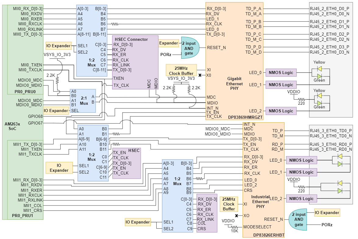
The AM263x Control Card makes use of two on-die programmable real-time unit and industrial communication subsystem's (PRU-ICSS) of the AM263x SoC to interface with two Ethernet PHY transceivers. There is a Gigabit Ethernet PHY transceiver (DP83869HMRGZT) connected to PRU0 of the SoC and an industrial Ethernet PHY transceiver (DP83826ERHBT) connected to PRU1. The ethernet data signals of each PHY are terminated to an RJ45 connector. The RJ45 connectors are used on the board for Ethernet 10/100/1000 (DP83869HMRGZT) and 10/100 (DP83826ERHBT) Mbps connectivity with integrated magnetic and LEDs for link and activity indication.
 Figure 4-11 ICSSM Overview
For the Gigabit Ethernet PHY:
- The Ethernet PHY requires three separate power sources. VDDIO is the 3.3 V, system generated analog supply. There are dedicated LDO's for the 1.1 V and 2.5 V supplies for the Ethernet PHY.
- The Ethernet PHY uses many functional pins as strap options to place the device into a specific mode of operation. Each functional pin has a default mode that is driven by an internal pull resistor.
- There is a 2:1 mux (TMUX154EDGSR) that controls the mapping of MDIO and MDC signals for the ethernet PHY's.
| SEL | Condition | Function |
|---|---|---|
| HIGH | AM263x SoC MDIO0 MDIO/MDC signals selected | A1/B1→A/B port |
| LOW | PRU MDIO/MDC signals selected | A0/B0→ A/B port |
- The Ethernet PHY uses many functional pins as strap options to place the device into a specific mode of operation. Each functional pin has a default mode that is driven by an internal pull resistor.
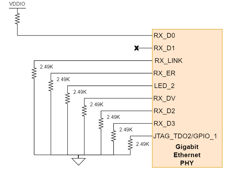
 Figure 4-12 PRU0 ICSS Gigabit Ethernet PHY
Strapping Resistors
Figure 4-12 PRU0 ICSS Gigabit Ethernet PHY
Strapping Resistors| Functional Pin | Default Mode | Mode in CC | Function |
|---|---|---|---|
| RX_D0 | 0 | 3 | PHY address: 0011 |
| RX_D1 | 0 | 0 | |
| JTAG_TDO/GGPIO_1 | 0 | 0 | RGMII to Copper |
| RX_D3 | 0 | 0 | |
| RX_D2 | 0 | 0 | |
| RX_LINK | 0 | 0 | Auto-negotiation, 1000/100/10 advertised, auto MDI-X |
| RX_ER | 0 | 0 | |
| LED_2 | 0 | 0 | |
| RX_DV | 0 | 0 | Port Mirroring Disabled |
For the Industrial Ethernet PHY transceiver:
- The Ethernet PHY requires two separate power sources. VDDIO is the 3.3 V, system generated analog supply. VSYS_IO_3V3 is the 3.3 V I/O supply.
- The Ethernet PHY is set to
ENHANCED mode by pulling the MODESELECT pin up to VDDIO.
- ENHANCED mode allows the DP83826E to support real-time Ethernet applications in addition to standard Ethernet applications.
- The Ethernet PHY uses many functional pins as strap options to place the device into a specific mode of operation. Each functional pin has a default mode that is driven by an internal pull resistor.
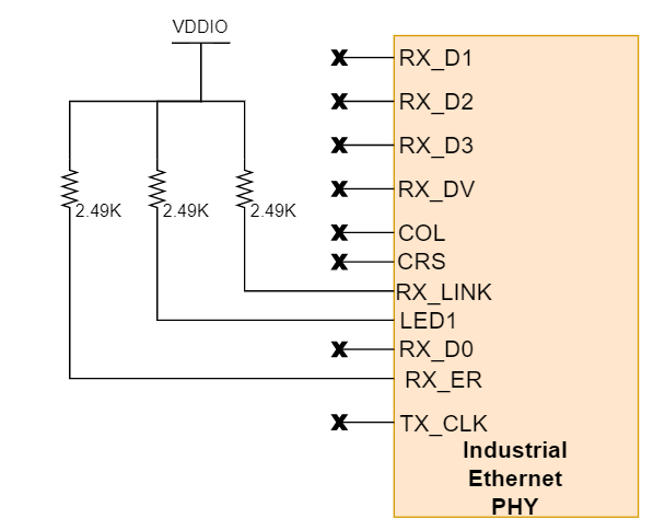
 Figure 4-13 PRU1 ICSS Industrial Ethernet
PHY Strapping Resistors
Figure 4-13 PRU1 ICSS Industrial Ethernet
PHY Strapping Resistors| Functional Pin | Default Mode | Mode in CC | Function |
|---|---|---|---|
| RX_D0 | 1 | 1 | Auto-negotiation enable |
| LED1 | 1 | 1 | Odd nibble detection enable |
| RX_LINK | 0 | 1 | PHY address: 001 |
| CRS | 0 | 0 | |
| COL | 0 | 0 | |
| TX_CLK | 0 | 0 | RMII Controller Mode |
| RX_ER | 0 | 1 | LED1 on pin 31 |
| RX_D3 | 0 | 0 | Fast link-drop disable |
| RX_D2 | 0 | 0 | MII MAC mode |
| RX_D1 | 0 | 0 | Auto MDIX enable |
| RX_DV | 0 | 0 | MDIX (applicable only when auto-MIDX is disabled) |
For both Ethernet PHY's:
- There are series termination resistors on the transmit and receive clock signals located near the AM263x SoC.
- The MDIO and Interrupt signals from the SoC to the PHY require 2.2KΩ pull up resistors to the I/O supply voltage for proper operation. The interrupt signal is driven by a GPIO signal that is mapped from the AM263x SoC.
- The reset signal for the Ethernet PHY is driven by a 2-input AND gate. The AND gate's inputs are a GPIO signal that is generated by the IO Expander and PORz.
- A 25 MHz clock is sourced from a four output clock buffer that has a 25 MHz oscillator as an input.
- There are three 1:2 muxes (TS3DDR3812RUAR) that control the mapping of ethernet signals from the SoC to either the Ethernet PHY's or the HSEC connector. The select logic for the three muxes is driven by two GPIO signals that are generated by the IO expander.
| Select Signal | Logic Level | Condition | Function |
|---|---|---|---|
| ICSSM1_MUX_SEL | LOW | PRU0 signals mapped to Ethernet PHY | A[n] → B[n] |
| HIGH | PRU0 signals mapped to HSEC | A[n] → C[n] | |
| ICSSM2_MUX_SEL | LOW | PRU1 signals mapped to Ethernet PHY | A[n] → B[n] |
| HIGH | PRU1 signals mapped to HSEC | A[n] → C[n] |