SPRUJ09D March   2022  – September 2023 AM2631 , AM2631-Q1 , AM2632 , AM2632-Q1 , AM2634 , AM2634-Q1 , AM263P4 , AM263P4-Q1


  1.   1
  2.   Abstract
  3.   Trademarks
  4. 1Preface: Read This First
    1. 2.1 Sitara MCU+ Academy
    2. 2.2 If You Need Assistance
    3. 2.3 Important Usage Notes
  5. 2Control Card Overview
    1. 3.1 Kit Contents
    2. 3.2 Key Features
    3. 3.3 Component Identification
    4. 3.4 HSEC 180-pin Control Card Docking Station
    5. 3.5 Compliance
  6. 3Board Setup
    1. 4.1 Power Requirements
      1. 4.1.1 Power Input Using USB Type-C Connector
      2. 4.1.2 Power Status LEDs
      3. 4.1.3 Power Tree
      4. 4.1.4 Power Sequence
    2. 4.2 Push Buttons
    3. 4.3 Boot Mode Selection
    4. 4.4 JTAG Path Selection
  7. 4Hardware Description
    1. 5.1  Functional Block Diagram
    2. 5.2  GPIO Mapping
    3. 5.3  Reset
    4. 5.4  Clock
    5. 5.5  Memory Interface
      1. 5.5.1 QSPI
      2. 5.5.2 Board ID EEPROM
    6. 5.6  Ethernet Interface
      1. 5.6.1 RGMII
      2. 5.6.2 PRU-ICSS
      3. 5.6.3 LED Indication in RJ45 Connector
    7. 5.7  I2C
    8. 5.8  Industrial Application LEDs
    9. 5.9  SPI
    10. 5.10 UART
    11. 5.11 MCAN
    12. 5.12 FSI
    13. 5.13 JTAG
    14. 5.14 Test Automation Header
    15. 5.15 LIN
    16. 5.16 MMC
    17. 5.17 ADC and DAC
    18. 5.18 HSEC Pinout and Pinmux Mapping
  8. 5References
    1. 6.1 References
    2. 6.2 Other TI Components Used in This Design
  9.   Revision History
  10.   A E2 Design Changes
  11.   B E1 HSEC Pinout Table

JTAG Path Selection

The AM263x Control Card allows for JTAG connections to the SoC through the on-board XDS110 or an external emulator via the HSEC docking station. A switch (SW5) is used to drive the select line of a mux (U19) to determine the JTAG path for the SoC. The following image shows proper switch position for SW5 for the two JTAG paths.
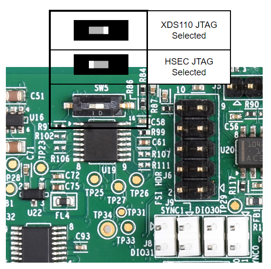
GUID-20211121-SS0I-5LCQ-NZ2Z-R2QJQXVVK8HH-low.png Figure 3-8 JTAG Path Switch Position