SPRUJ12F August 2021 – January 2024 AM2431 , AM2432 , AM2434
- 1
- Abstract
- Trademarks
- 1Preface: Read This First
- 2Kit Overview
- 3Board Setup
-
4Hardware Description
- 4.1 Functional Block Diagram
- 4.2 BoosterPack Headers
- 4.3 GPIO Mapping
- 4.4 Reset
- 4.5 Clock
- 4.6 Memory Interface
- 4.7 Ethernet Interface
- 4.8 USB 2.0 Interface
- 4.9 I2C Interface
- 4.10 Industrial Application LEDs
- 4.11 UART Interface
- 4.12 eQEP Interface
- 4.13 CAN Interface
- 4.14 FSI Interface
- 4.15 JTAG Emulation
- 4.16 Test Automation Interface
- 4.17 SPI Interface
- 5References
- A E3 Design Changes
- B Revision A Design Changes
- Revision History
4.6.2 Board ID EEPROM
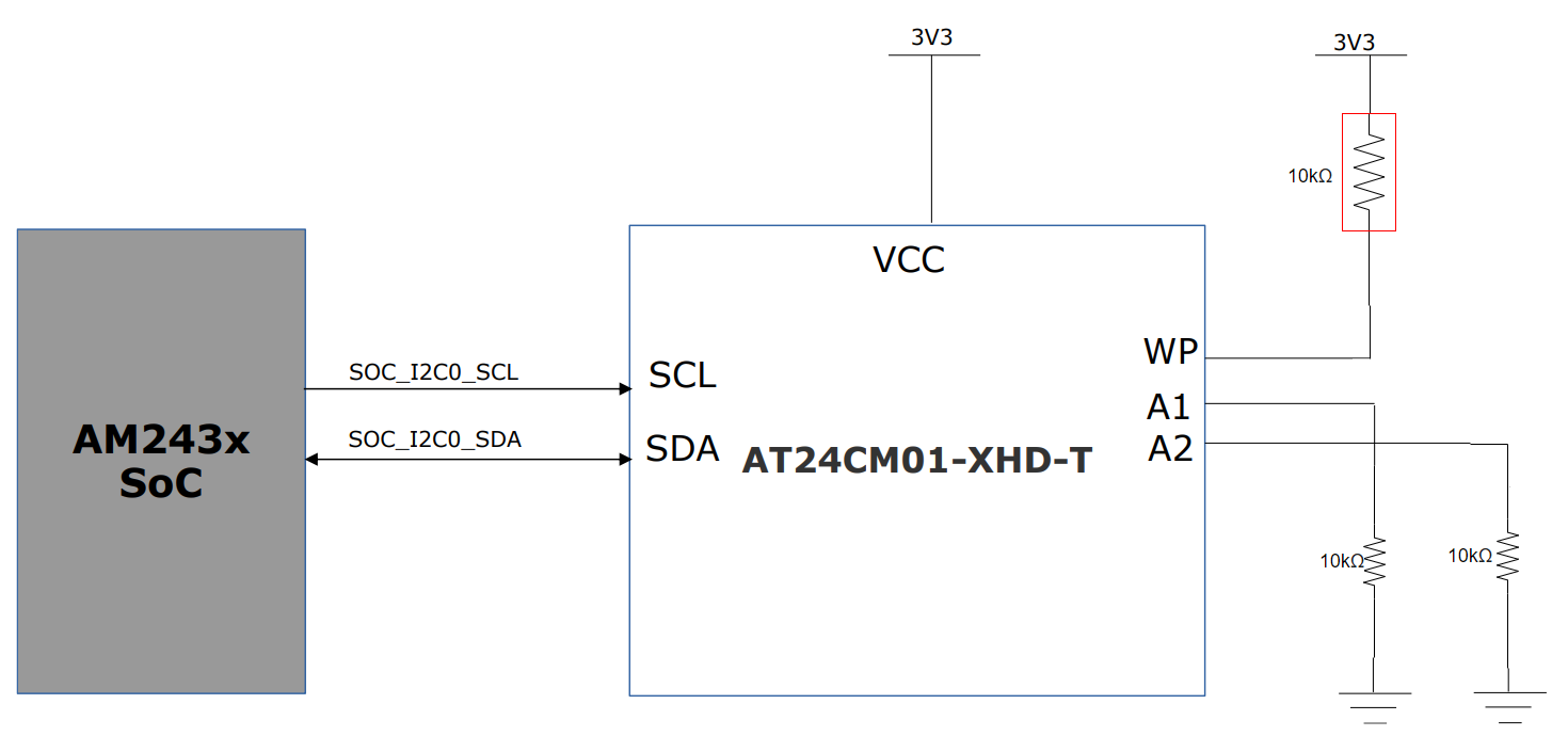
The AM243x LaunchPad has a 1 Mbit I2C EEPROM for board ID information. The board ID memory is configured to respond to the I2C address 0X50 by connecting the address pins (A0, A1) to ground and programmed with the header description. This EEPROM (AT24CM01-XHD-T from Microchip) is interfaced to the I2C0 port of the SoC. When the WP pin is connected directly to VCC then all write operations to the protected memory are inhibited. The mounted resistor is shown inside of the red box in Figure 4-8. For normal operation, the WP pin can be left floating by isolating the resistor shown in the red box (R89).
 Figure 4-8 Board ID EEPROM
| Header | Field Name | # Bytes | Offset | Field Value | Field Type | Description |
|---|---|---|---|---|---|---|
| EE3355AA | MAGIC | 4 | 0000 | 0xEE3355AA | HEX | Magic Number |
| TYPE | 1 | 0004 | 0x01 | HEX | Fixed length and variable position board ID header | |
| 2 | 0005 | F7 | HEX | Size of payload bytes following this field including end_list byte | ||
| BRD_INFO | TYPE | 1 | 0007 | 0x10 | HEX | Board Info header identifier |
| Length | 2 | 0008 | 2E | HEX | offset to next header | |
| Board_Name | 16 | 000A | AM243-LPEVM | CHAR | ||
| Design_Rev | 2 | 001A | E2 | CHAR | ||
| PROC_Nbr | 4 | 001C | 109 | CHAR | PROC number from central EVM | |
| Variant | 2 | 0020 | 01 | CHAR | ||
| PCB_Rev | 2 | 0022 | E2 | CHAR | ||
| SCHBOM_Rev | 2 | 0024 | 00 | CHAR | Used for schematic revision extension - A, B, C etc. Schematic/BoM revision will be Design_Rev+SCHBOM_Rev | |
| SWR_Rev | 2 | 0026 | 01 | CHAR | 1 is first software release | |
| VendorID | 2 | 0028 | 01 | CHAR | 1 is Mistral | |
| Build_Week | 2 | 002A | 20 | CHAR | Filled in by Mistral | |
| Build_Year | 2 | 002C | 21 | CHAR | 2021 | |
| BoardID | 6 | 002E | 0 | CHAR | Legacy apps part number. Not used for recent boards. Will be marked as 0 | |
| Serial_Nbr | 4 | 0034 | xxxx | CHAR | Filled in by Mistral | |
| MAC_ADDR | TYPE | 1 | 0038 | 0x13 | HEX | MAC address header identifier |
| LENGTH | 2 | 0039 | 0xC2 | HEX | Size of payload | |
| MAC control | 2 | 003B | 0x10 | HEX | MAC header control word | |
| MAC_adrs | 192 | 003D | xxxx | HEX | Will have three valid MAC addresses | |
| END_LIST | TYPE | 1 | 00FD | 0xFE | HEX | End Marker |