SPRUJ51 june 2023
- 1
- 1Abstract
- 2EVM Revisions and Assembly Variants
- Trademarks
-
3System Description
- 3.1 Key Features
- 3.2 Functional Block Diagram
- 3.3 AM62x-Low Power SK EVM Interface Mapping
- 3.4 Power ON OFF Procedures
- 3.5
Peripheral and Major Component Description
- 3.5.1 Clocking
- 3.5.2 Reset
- 3.5.3 OLDI Display Interface
- 3.5.4 CSI Interface
- 3.5.5 Audio Codec Interface
- 3.5.6 HDMI Display Interface
- 3.5.7 JTAG Interface
- 3.5.8 Test Automation Header
- 3.5.9 UART Interface
- 3.5.10 USB Interface
- 3.5.11 Memory Interfaces
- 3.5.12 Ethernet Interface
- 3.5.13 GPIO Port Expander
- 3.5.14 GPIO Mapping
- 3.5.15 Power
- 3.5.16 AM62x-Low Power SK EVM User Setup and Configuration
- 3.5.17 Expansion Headers
- 3.5.18 Push Buttons
- 3.5.19 I2C Address Mapping
- 4Known Issues and Modifications
- 5Revision History
- 6IMPORTANT NOTICE AND DISCLAIMER
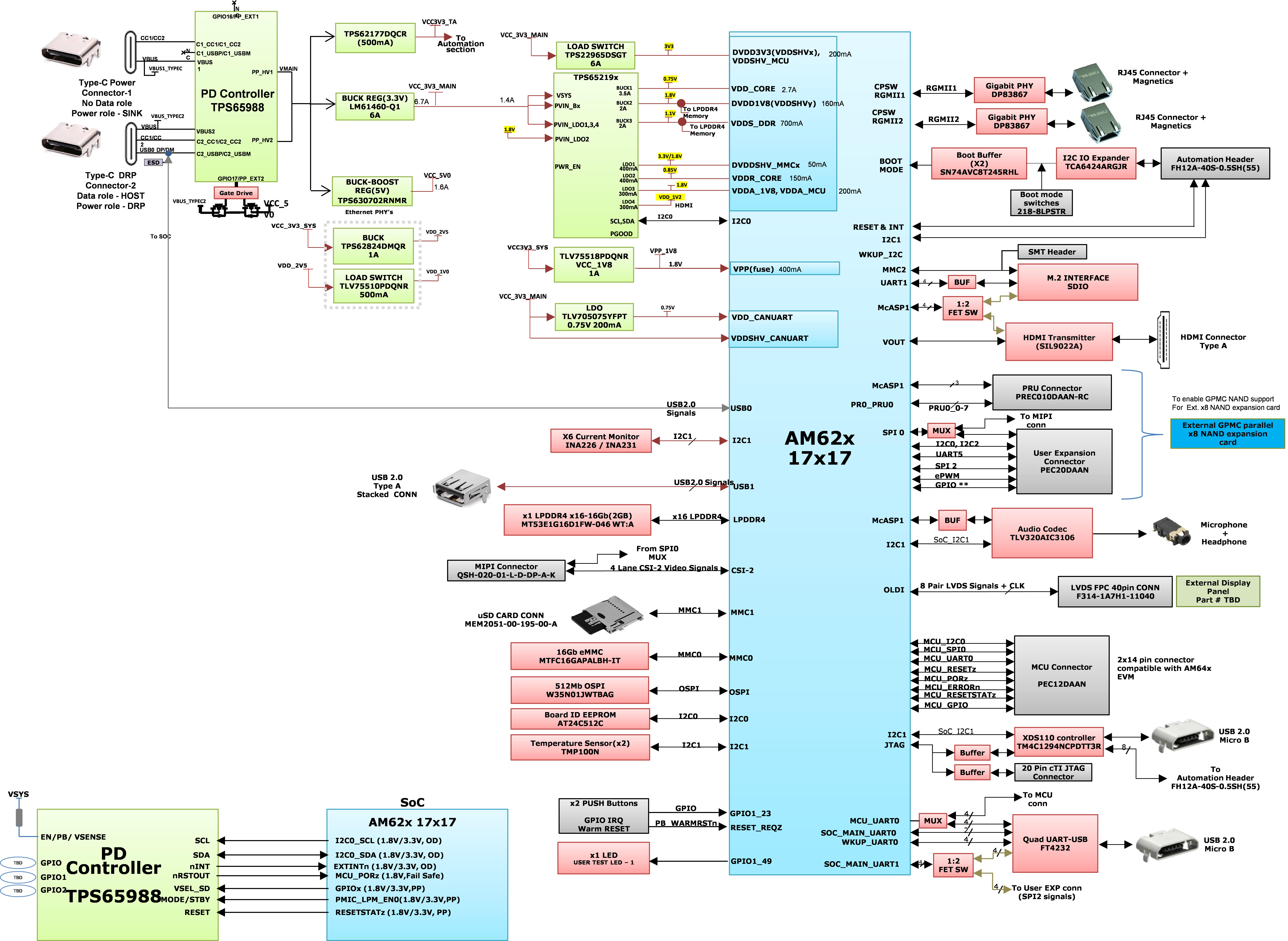
3.2 Functional Block Diagram
The functional block diagram of the AM62x-Low Power SK EVM is shown below.
 Figure 3-4 Functional Block
Diagram