SPRUJ67A October 2022 – October 2023
2.3 LCD and EVM Connectivity
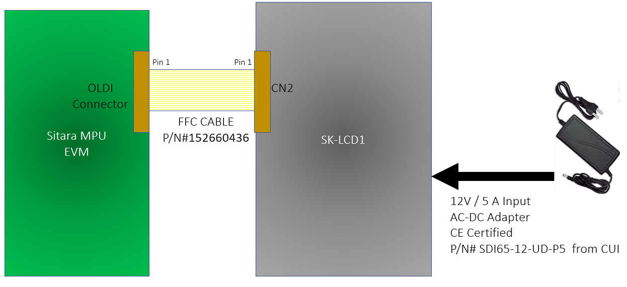
The LCD and EVM shall be interfaced using 40 pin opposite side contacts flat flex cable (MFR: Molex, PN: 152660436). The flat flex cable shall be connected to CN2 connector of the LCD and OLDI connector of the EVM (ref des varies in different EVM).
The EVM shall be assembled to the LCD kit using the standoff and fasteners provided in the box.
Note: Make sure that the pin 1 connection
on same side of the cable.
TI recommends using 12 V external power adapter to power up the LCD MFR: CUI, PN: SDI65-12-UD-P5.
 Figure 2-5 LCD and EVM Connection
Diagram
 Figure 2-6 LCD and EVM Assembly
Table 2-1 LCD and EVM Connector Pinout
| Pin Number | EVM OLDI Connector | LCD Connector |
|---|---|---|
| 1 | VCC_3V3_SYS | EEPROM_VDD |
| 2 | SOC_I2C0_SCL | I2C_SCL |
| 3 | SOC_I2C_SDA | I2C_SDA |
| 4 | NC | NC |
| 5 | NC | NC |
| 6 | GND | GND |
| 7 | GND | GND |
| 8 | OLDI_RESET_N | PCT_RST |
| 9 | TS_INT# | PCT_INT |
| 10 | GND | GND |
| 11 | CH1_LVDS_A0N | OIN0- |
| 12 | CH1_LVDS_A1P | OIN0+ |
| 13 | GND | GND |
| 14 | CH1_LVDS_A1N | OIN1- |
| 15 | CH1_LVDS_A1P | OIN1+ |
| 16 | GND | GND |
| 17 | CH1_LVDS_CLKN | OCLK- |
| 18 | CH1_LVDS_CLKP | OCLK+ |
| 19 | GND | GND |
| 20 | CH1_LVDS_A2N | OIN2- |
| 21 | CH1_LVDS_A2P | OIN2+ |
| 22 | GND | GND |
| 23 | CH1_LVDS_A3N | OIN3- |
| 24 | CH1_LVDS_A3P | OIN3+ |
| 25 | GND | GND |
| 26 | CH2_LVDS_A0N | EIN0- |
| 27 | CH2_LVDS_A0P | EIN0+ |
| 28 | GND | GND |
| 29 | CH2_LVDS_A1N | EIN1- |
| 30 | CH2_LVDS_A1P | EIN1+ |
| 31 | GND | GND |
| 32 | CH2_LVDS_CLKN | ECLK- |
| 33 | CH2_LVDS_CLKP | ECLK+ |
| 34 | GND | GND |
| 35 | CH2_LVDS_A2N | EIN2- |
| 36 | CH2_LVDS_A2P | EIN2+ |
| 37 | GND | GND |
| 38 | CH2_LVDS_A3N | EIN3- |
| 39 | CH2_LVDS_A3P | EIN3+ |
| 40 | GND | GND |