SPRUJ73 December 2023
2.5.4 TRACE/GPMC Muxing Scheme
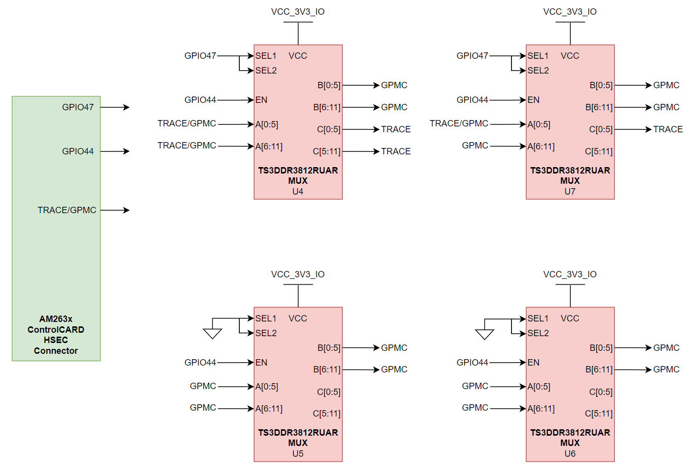
On the AM263x SoC, the GPMC signals are pinmuxed with the TRACE data signals. Four TS3DDR3812RUAR 12-channel high speed multiplexers are used to separate the signals and enables both TRACE emulation and GPMC usage on the AM263x controlCARD Docking Station.
 Figure 2-10 TRACE/GPMC Signal
Muxing
Figure 2-10 TRACE/GPMC Signal
MuxingGPIO44 from the AM263x SoC (HSEC pin 51) is the enable bit on all multiplexers. GPIO47 from the AM263x SoC (HSEC pin 50) is connected to both select bits on U4 and U7. By default, these signals are pulled up to the 3.3V IO rail, with the default signal output being the TRACE signals. The GPMC driver in the AM263x MCU+ SDK pulls GPIO47 low to allow the multiplexers to pass the GPMC signals.
U4 and U7 multiplex both TRACE and GPMC signals, while U5 and U6 do not have configurable select bits and only pass GPMC signals. There are more GPMC signals than TRACE signals, and this keeps timing consistent across all GPMC nets.
| EN | SEL1 | SEL2 | Mux Function | controlCARD Signal Routing |
|---|---|---|---|---|
| L | X | X | A0 to A11, B0 to B11, and C0 to C11 are Hi-Z | N/A |
| H | L | L | A0 to A5 = B0 to B5 A6 to A11 = B6 to B11 |
GPMC Selected |
| H | L | H | A0 to A5 = B0 to B5 A6 to A11 = C6 to C11 |
N/A |
| H | H | L | A0 to A5 = C0 to C5 A6 to A11 = B6 to B11 |
N/A |
| H | H | H | A0 to A5 = C0 to C5 A6 to A11 = C6 to C11 |
TRACE Selected (default) |