SPRUJ74 January   2023


  1.   Trademarks
  2. 1Introduction
    1. 1.1 Key Features
    2. 1.2 Thermal Compliance
    3. 1.3 EMC, EMI, and ESD Compliance
  3. 2QP-ENET Board Identification and Installation
    1. 2.1 QP-ENET Board Component Identification
    2. 2.2 Interfacing QP-ENET Expansion Board with J784S4XG01EVM Board
      1. 2.2.1 Detailed Board Assembly Procedure (J784S4XG01EVM)
  4. 3QP-ENET Expansion Board Hardware Architecture
    1. 3.1 QP-ENET Expansion Board Hardware Top Level Diagram
    2. 3.2 Expansion Connectors
    3. 3.3 Board ID EEPROM
    4. 3.4 Ethernet Interface
      1. 3.4.1 Quad Port SGMII PHY Default Configuration
      2. 3.4.2 SGMII Clocking Scheme
        1. 3.4.2.1 Main Clock
        2. 3.4.2.2 Optional Clock
      3. 3.4.3 Ethernet Port LED Indication
      4. 3.4.4 Reset and Power-down Signals
  5. 4Revision History
  6.   A Appendix
    1.     A.1 Appendix – I (Interface Mapping)
    2.     A.2 Appendix – II (QP-ENET Board GPIO Mapping)

QP-ENET Expansion Board Hardware Top Level Diagram

The generic functional block diagram of the QP-ENET Expansion Board is shown below.
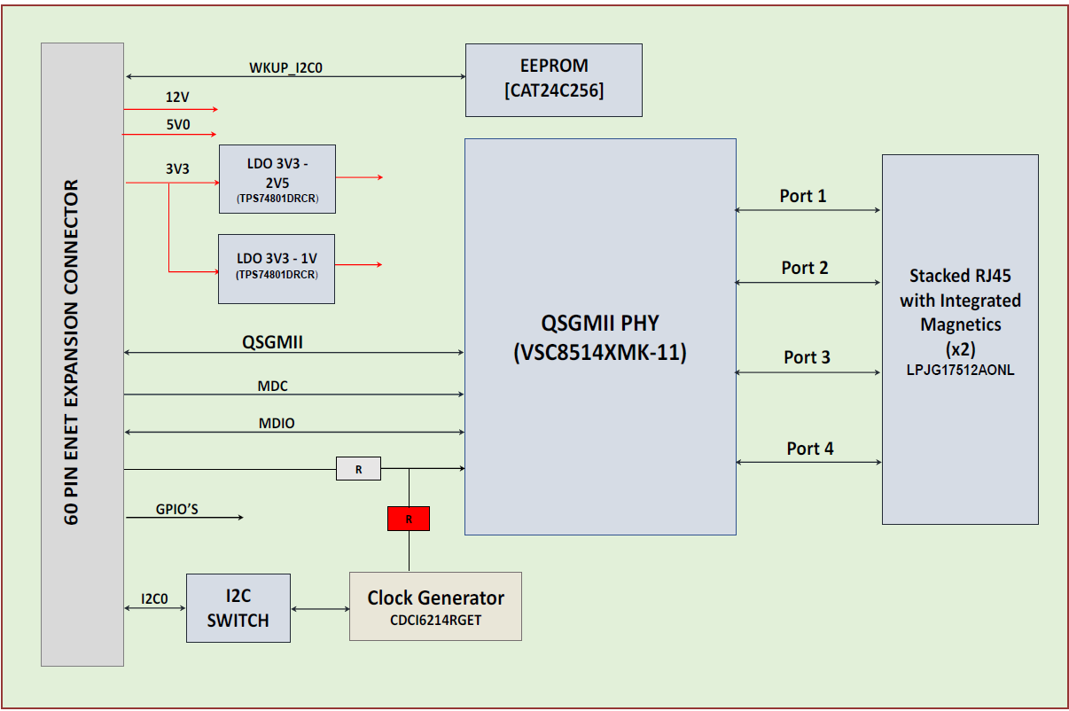
GUID-BA1A577D-E8E7-4DAB-B615-3918FA299DFC-low.png Figure 3-1 Functional Block Diagram of QP-ENET Expansion Board