SPRUJ81 February 2023 AM62A3 , AM62A3-Q1 , AM62A7 , AM62A7-Q1
10 Power Decoupling
The middle priority interfaces and the power distribution planes and pours are routed next after the SerDes and DDR interfaces. TI recommends completing all SerDes and DDR routing before continuing with other interfaces. The power distribution planes and pours and all of the decoupling must be placed before PCB simulations are executed for the SerDes and DDR routes, as these can influence the return currents for the high-speed interfaces. The highest speed source-synchronous interfaces, such as RGMII and QSPI, may also require simulation, so these may also need to be completed at this time.
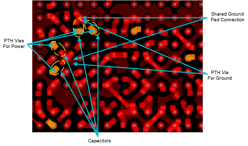
Special care is needed for the 1-uF output capacitors connected to the CAP_VDDS* BGA pins on the AM62Ax device. These capacitors should be placed as close to the pin as possible, and a low inductance path should be present between the CAP_VDDS BGA pin and the supply pad on the capacitor. The layout used on the CAP_VDDS0, CAP_VDDS1, CAP_VDDS5, and CAP_VDDS6 nets on the AM62Ax board is shown below in Figure 10-1. Note the sharing of the GND pad of the capacitors with other capacitors in the vicinity, which allows saving routing resources. Also, it is important to keep the PTH vias for the capacitor power and GND pad connections as close to each other as possible to minimize the loop inductance.
 Figure 10-1 Output Capacitor Placement for
CAP_VDDS Nets
Figure 10-1 Output Capacitor Placement for
CAP_VDDS NetsThis placement can be improved if the capacitors can be placed directly under the SoC. The decoupling capacitors for the VDD_CORE and VDDS_DDR supplies should also receive the same priority as those on the CAP_VDDS* pins and should be placed under the socket, with minimum inductance connections to the respective BGA pins on the AM62Ax device.