SPRUJ85 April 2024
ADVANCE INFORMATION
- 1
- Description
- Key Features
- 1LaunchPad Module Overview
-
2Hardware Description
- 3.1 Board Setup
- 3.2 Functional Block Diagram
- 3.3 GPIO Mapping
- 3.4 Reset
- 3.5 Clock
- 3.6 Memory Interface
- 3.7 Ethernet Interface
- 3.8 I2C
- 3.9 Industrial Application LEDs
- 3.10 SPI
- 3.11 UART
- 3.12 MCAN
- 3.13 FSI
- 3.14 JTAG
- 3.15 TIVA and Test Automation Header
- 3.16 LIN
- 3.17 MMC
- 3.18 ADC and DAC
- 3.19 EQEP and SDFM
- 3.20 EPWM
- 3.21 BoosterPack Headers
- 3.22 Pinmux Mapping
- 3Additional Information
- 4References
- 5Revision History
2.12 MCAN
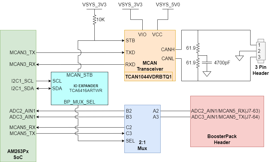
The LaunchPad is equipped with a single MCAN Transceiver (TCAN1044VDRBTQ1) that is connected to the MCAN3 interface of the AM263Px SoC. The MCAN Transceiver has two power inputs, VIO is the transceiver 3.3V system level shifting supply voltage and VCC is the transceiver 5V supply voltage. The SoC CAN data transmit data input is mapped to TXD of the transceiver and the CAN receive data output of the transceiver is mapped to the MCAN RX signal of the SoC.
 Figure 2-21 MCAN Transceiver and BoosterPack Header
The system has a 120Ω split termination on the CANH and CANL signals to improve EMI performance. Split termination improves the electromagnetic emissions behavior of the network by eliminating fluctuations in the bus common-mode voltages at the start and end of message transmissions.
The low and high level CAN bus input output lines are terminated to a three pin header.
The standby control signal is an AM263Px SoC GPIO signal. The STB control input has a pullup resistor that is used to have the transceiver be in low-power standby mode to prevent excessive system power. Below is a table that shows the operating modes of the MCAN transceiver based on the STB control input logic.
| STB | Device Mode | Driver | Receiver | RXD Pin |
|---|---|---|---|---|
| High | Low current standby mode with bus wake-up | Disabled | Low-power receiver and bus monitor enable | High (recessive) until valid WUP is received |
| Low | Normal Mode | Enabled | Enabled | Mirrors bus state |
MCAN5 is routed to the BoosterPack Header via a 2:1 mux. The mux selects whether ADC inputs or MCAN signals are mapped to the BoosterPack Header.
| BP_MUX_SEL | Condition | Function of Mux |
|---|---|---|
| LOW | ADC Inputs Selected | Port A ↔ Port B |
| HIGH | MCAN TX/RX Selected | Port A ↔ Port C |