SPRUJ85 April 2024
ADVANCE INFORMATION
- 1
- Description
- Key Features
- 1LaunchPad Module Overview
-
2Hardware Description
- 3.1 Board Setup
- 3.2 Functional Block Diagram
- 3.3 GPIO Mapping
- 3.4 Reset
- 3.5 Clock
- 3.6 Memory Interface
- 3.7 Ethernet Interface
- 3.8 I2C
- 3.9 Industrial Application LEDs
- 3.10 SPI
- 3.11 UART
- 3.12 MCAN
- 3.13 FSI
- 3.14 JTAG
- 3.15 TIVA and Test Automation Header
- 3.16 LIN
- 3.17 MMC
- 3.18 ADC and DAC
- 3.19 EQEP and SDFM
- 3.20 EPWM
- 3.21 BoosterPack Headers
- 3.22 Pinmux Mapping
- 3Additional Information
- 4References
- 5Revision History
2.18 ADC and DAC
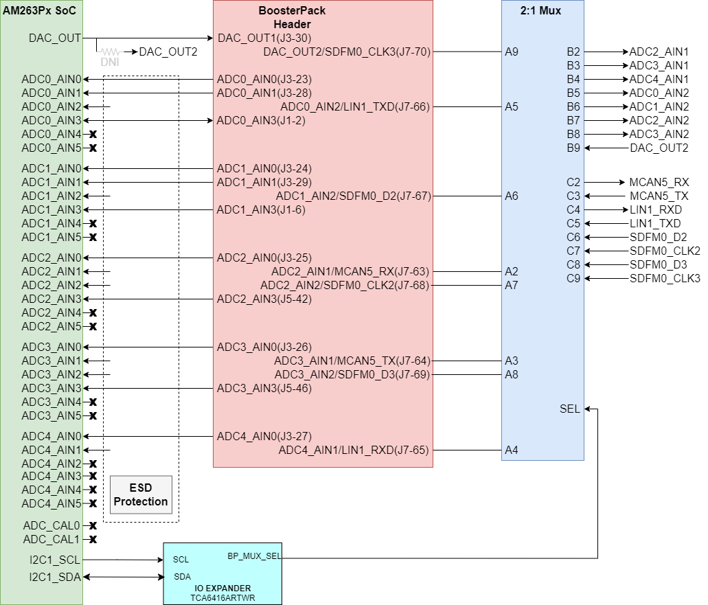
The AM263Px LaunchPad maps 20 ADC inputs to the BoosterPack header. All of the ADC inputs that are used in the LaunchPad are ESD protected.
 Figure 2-27 ADC/DAC Signal Pathing
Seven of the ADC inputs and one instance of the DAC_OUT signal is routed to a 2:1 mux (TS3DDR3812RUAR) to offer alternate BoosterPack functionality. The select line of the mux is driven by an AM263Px SoC GPIO signal.
| BP_MUX_SEL | Condition | Funciton of Mux |
|---|---|---|
| LOW | ADC input/DAC_OUT Selected | Port A ↔ Port B |
| HIGH | Alternate BP functionality Selected | Port A ↔ Port C |
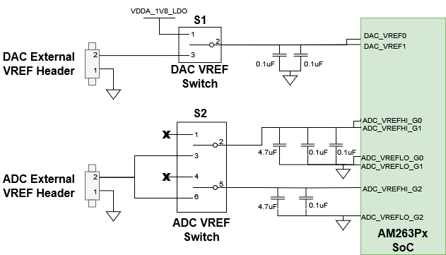
The ADC and DAC require a voltage reference. The AM263Px LaunchPad has two switches that allow the user to switch between the DAC and ADC VREF source.

Figure 2-28 ADC and DAC VREF Switches
The DAC VREF Switch (S1) is a single pole double throw switch that controls the input of the ADC VREF inputs of the AM263Px SoC.
| DAC VREF Switch Position | Reference Selection |
|---|---|
| Pin 1-2 | AM263Px on-die LDO |
| Pin 2-3 | External DAC VREF Header |
The ADC VREF Switch (S2) contains two single pole double throw switches that controls the input of the ADC VREF inputs of the AM263Px SoC.
| ADC VREF Switch Position | Reference Selection |
|---|---|
| Pin 1-2 | OPEN - Allow for reference to be AM263Px on-die LDO reference |
| Pin 2-3 | External ADC VREF Header |
| Pin 4-5 | OPEN - Allow for reference to be AM263Px on-die LDO reference |
| Pin 5-6 | External ADC VREF Header |