SPRUJ85 April 2024
ADVANCE INFORMATION
- 1
- Description
- Key Features
- 1LaunchPad Module Overview
-
2Hardware Description
- 3.1 Board Setup
- 3.2 Functional Block Diagram
- 3.3 GPIO Mapping
- 3.4 Reset
- 3.5 Clock
- 3.6 Memory Interface
- 3.7 Ethernet Interface
- 3.8 I2C
- 3.9 Industrial Application LEDs
- 3.10 SPI
- 3.11 UART
- 3.12 MCAN
- 3.13 FSI
- 3.14 JTAG
- 3.15 TIVA and Test Automation Header
- 3.16 LIN
- 3.17 MMC
- 3.18 ADC and DAC
- 3.19 EQEP and SDFM
- 3.20 EPWM
- 3.21 BoosterPack Headers
- 3.22 Pinmux Mapping
- 3Additional Information
- 4References
- 5Revision History
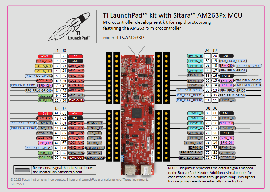
2.21 BoosterPack Headers
 Figure 2-31 AM263Px LaunchPad BoosterPack Pinout
Note: This pinout represents the default signals mapped to the BoosterPack Header. Additional signal options for each header are available through Pinmux Mapping. Two signals for one pin represents an externally muxed option
The AM263Px LaunchPad supports two fully independent BoosterPack XL connectors. BoosterPack site #1 (J1/J3, J2/J4) is located in between the SoC and the micro-B USB Connector. BoosterPack site #2 (J5/J7, J6/J8) is located in between the SoC and the RJ45 connectors. Each GPIO has multiple functions available through the GPIO mux. The signals connected from the SoC to the BoosterPack headers include:
- Various ADC inputs
- DAC outouts
- UART5
- Various GPIO signals
- SPI0 and SPI1
- I2C1 and I2C3
- Various EPWM channels
- LIN1 and LIN2
- MCAN1
- SDFM0