SPRUJ85 April 2024
ADVANCE INFORMATION
- 1
- Description
- Key Features
- 1LaunchPad Module Overview
-
2Hardware Description
- 3.1 Board Setup
- 3.2 Functional Block Diagram
- 3.3 GPIO Mapping
- 3.4 Reset
- 3.5 Clock
- 3.6 Memory Interface
- 3.7 Ethernet Interface
- 3.8 I2C
- 3.9 Industrial Application LEDs
- 3.10 SPI
- 3.11 UART
- 3.12 MCAN
- 3.13 FSI
- 3.14 JTAG
- 3.15 TIVA and Test Automation Header
- 3.16 LIN
- 3.17 MMC
- 3.18 ADC and DAC
- 3.19 EQEP and SDFM
- 3.20 EPWM
- 3.21 BoosterPack Headers
- 3.22 Pinmux Mapping
- 3Additional Information
- 4References
- 5Revision History
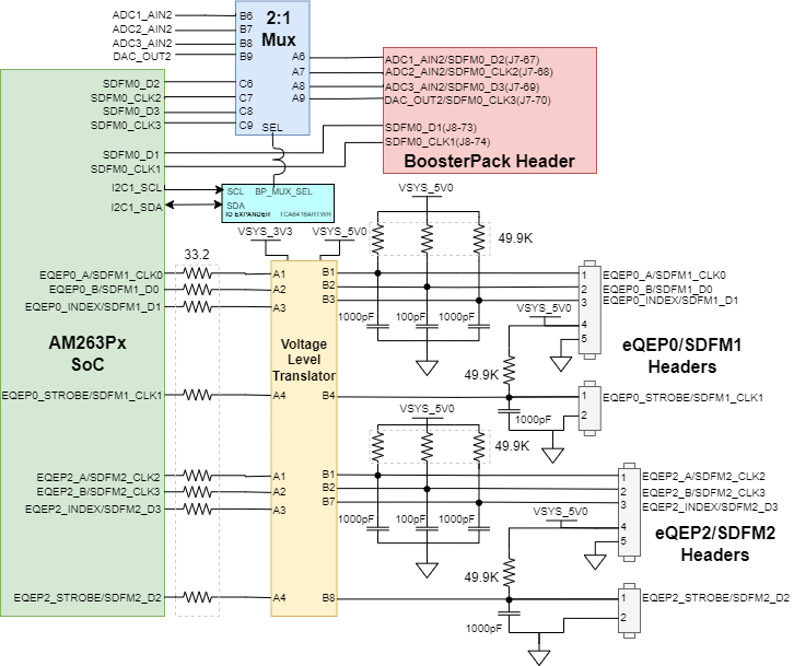
2.19 EQEP and SDFM
The AM263Px LaunchPad internally muxes the eQEP and SDFM signals. The eQEP0 and SDFM1 instances of the AM263Px are terminated to two headers (J24, J15). The eQEP2 and SDFM2 instances of the AM263Px are terminated to two headers (J25, J16).
 Figure 2-29 EQEP and SDFM Signal Mapping
All eQEP signals have series termination resistors between the AM263Px SoC and the Voltage Level Translator (TXB0108RGYR). The voltage level shifter is responsible for translating the 3.3V to 5V.
SDFM0 is mapped to the BoosterPack Header rather than an independent header. Four of the SDFM0 signals are routed through a 2:1 mux to offer alternate BoosterPack functionality. The select line of the mux is driven by an AM263Px SoC GPIO signal.
Table 2-23 SDFM0 Mux
| BP_MUX_SEL | Condition | Function of Mux |
|---|---|---|
| LOW | Alternate BP functionality Selected | Port A ↔ Port B |
| HIGH | SDFM0 Selected | Port A ↔ Port C |