SPRUJ85 April 2024
ADVANCE INFORMATION
- 1
- Description
- Key Features
- 1LaunchPad Module Overview
-
2Hardware Description
- 3.1 Board Setup
- 3.2 Functional Block Diagram
- 3.3 GPIO Mapping
- 3.4 Reset
- 3.5 Clock
- 3.6 Memory Interface
- 3.7 Ethernet Interface
- 3.8 I2C
- 3.9 Industrial Application LEDs
- 3.10 SPI
- 3.11 UART
- 3.12 MCAN
- 3.13 FSI
- 3.14 JTAG
- 3.15 TIVA and Test Automation Header
- 3.16 LIN
- 3.17 MMC
- 3.18 ADC and DAC
- 3.19 EQEP and SDFM
- 3.20 EPWM
- 3.21 BoosterPack Headers
- 3.22 Pinmux Mapping
- 3Additional Information
- 4References
- 5Revision History
2.16 LIN
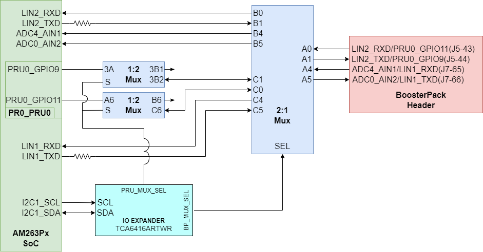
The AM263Px LaunchPad supports Local Interconnect Network communication with two LIN instances mapped to the BoosterPack header.
Note: The AM263Px does not have an onboard LIN Transceiver
 Figure 2-25 LIN Instances to BoosterPack Header
Both LIN instances are mapped to the alternate BoosterPack function 2:1 mux. The alternate BoosterPack function mux also has mappings for ADC inputs and PRU0 GPIO signals.
Table 2-19 LIN 2:1 Mux
| PRU_MUX_SEL | BP_MUX_SEL | Function of 2:1 Mux | Signals to BP Header |
|---|---|---|---|
| HIGH | LOW | Port A ↔ Port B | LIN2TX/RX, ADC4_AIN1, ADC0_AIN2 |
| HIGH | HIGH | Port A ↔ Port C | PRU GPIO11/9, LIN1TX/RX |
| LOW | LOW | Port A ↔ Port B | LIN2TX/RX, ADC4_AIN1, ADC0_AIN2 |
| LOW | HIGH | Port A ↔ Port C | NC, NC, LIN1 TX/RX |