SPRUJ85A April 2024 – August 2024
PRODUCTION DATA
- 1
- Description
- 1Key Features
- 2LaunchPad Module Overview
-
3Hardware Description
- 4.1 Board Setup
- 4.2 Functional Block Diagram
- 4.3 GPIO Mapping
- 4.4 Reset
- 4.5 Clock
- 4.6 Memory Interfaces
- 4.7 Ethernet Interface
- 4.8 I2C
- 4.9 Industrial Application LEDs
- 4.10 SPI
- 4.11 UART
- 4.12 MCAN
- 4.13 FSI
- 4.14 JTAG
- 4.15 TIVA and Test Automation Header
- 4.16 LIN
- 4.17 ADC and DAC
- 4.18 EQEP and SDFM
- 4.19 EPWM
- 4.20 BoosterPack Headers
- 4.21 Pinmux Mapping
- 4Additional Information
- 5References
- 6Revision History
3.4 Reset
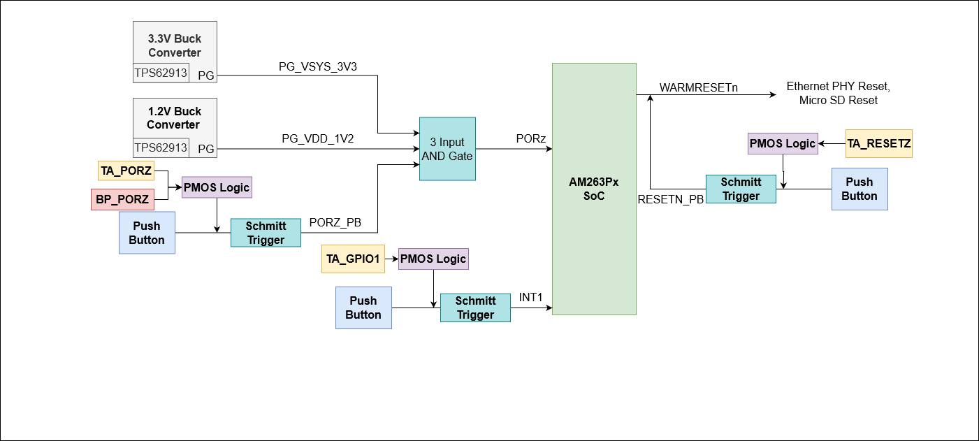
Figure 3-9 shows the reset architecture of the AM263Px LaunchPad

Figure 3-9 Reset Architecture
The AM263Px LaunchPad has the following resets:
- PORz is the Power On Reset
- WARMRESETn is the warm reset

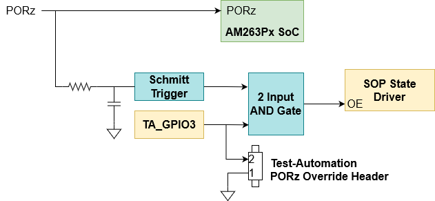
Figure 3-10 PORZ Reset Signal Tree
The PORz signal is driven by a 3-input AND gate that generates a power on reset for the MAIN domain when:
- The 3.3V buck converter (TPS62913) power good output is driven low by having an output voltage that is below the power-good threshold.
- The 1.2V buck converter (TPS62913) power good output is driven low by having an output voltage that is below the power-good threshold.
- The user push button (SW2) is pressed.
- A P-Channel MOSFET gate's signal is logic LOW which causes VGS of the PMOS to be less than zero and so the PORz signal connects to the PMOS drain which is tied directly to ground. The signals that can create the logic LOW input to the PMOS gate are:
- TA_PORZ output from the Test Automation header
- BP_PORZ output from either of the BoosterPack sites.
The PORz signal is tied to:
- AM263Px SoC PORz input
- Boot mode State Driver(U4)'s output enable input
- There is an RC filter to create a 1ms delay from GND to 3.0V such that the SOP State Driver's output enable input is low longer than the required SOP hold time following a PORz de-assertion.
There is a Test-Automation PORz Override header that enables the ability to hold TA_GPIO3 low when a jumper is installed. This enables the boot mode Control from the Test Automation Header.

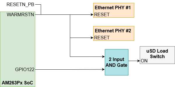
Figure 3-11 WARMRESETn Reset Signal Tree
The WARMRESETn signal creates a warm reset to the MAIN domain when:
- The user push button (SW3) is pressed.
- The Test Automation Header outputs a logic LOW signal (TA_RESETz) to a P-Channel MOSFET gate which causes VGS of the PMOS to be less than zero and so the RESETz signal connects to the PMOS drain which is tied directly to ground.
The WARMRESETn signal is tied to:
- AM263Px SoC WARMRESETN output
- RESETN_PB signal that is created from push button + PMOS logic
- Micro SD Load Switch control input via a 2 input AND Gate with an AM263Px SoC driven GPIO signal (GPIO122)
- Both Ethernet PHY's reset input
The AM263Px LaunchPad also has an external interrupt to the SoC , INT1, that occurs when:
- The user push button (SW4) is pressed.
- The Test Automation Header outputs a logic LOW signal (TA_GPIO1) to a P-Channel MOSFET gate which causes VGS of the PMOS to be less than zero and so the INTn signal connects to the PMOS drain which is tied directly to ground.