SPRUJ85A April 2024 – August 2024
PRODUCTION DATA
- 1
- Description
- 1Key Features
- 2LaunchPad Module Overview
-
3Hardware Description
- 4.1 Board Setup
- 4.2 Functional Block Diagram
- 4.3 GPIO Mapping
- 4.4 Reset
- 4.5 Clock
- 4.6 Memory Interfaces
- 4.7 Ethernet Interface
- 4.8 I2C
- 4.9 Industrial Application LEDs
- 4.10 SPI
- 4.11 UART
- 4.12 MCAN
- 4.13 FSI
- 4.14 JTAG
- 4.15 TIVA and Test Automation Header
- 4.16 LIN
- 4.17 ADC and DAC
- 4.18 EQEP and SDFM
- 4.19 EPWM
- 4.20 BoosterPack Headers
- 4.21 Pinmux Mapping
- 4Additional Information
- 5References
- 6Revision History
3.6.1 OSPI
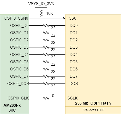
The AM263Px LaunchPad has a 256 Mb OSPI Flash memory device (IS25LX256-LHLE), which is connected to the OSPI0 interface of the AM263Px SoC. The OSPI supports single data rates and double data rates with memory speeds up to 133MHz. The OSPI flash is powered by the 3.3V system supply.
The OSPI0_D0/D1 signals are also used for boot mode control logic. There are 10KΩ resistors used to isolate the boot mode control logic after the value is latched.
 Figure 3-13 OSPI Flash Interface
AM263P_OSPI0_DQS(UART1_RXD) and AM263P_OSPI0_LBCLK(UART1_TXD) net names are wrongly swapped in the schematics. As per datasheet OSPI0_DQS must be connected to M3 ball pin and OSPI0_LBCLKO must be connected to L3 Ball pin.
Refer to OSPI DQS and LBCLK nets swap for more details.