SPRUJ86C October 2023 – August 2024 AM263P2 , AM263P4 , AM263P4-Q1
- 1
- Description
- Features
- 4
- 1Evaluation Module Overview
-
2Hardware
- 2.1 Component Identification
- 2.2 Power Requirements
- 2.3 Functional Block Diagram
- 2.4 Reset
- 2.5 Clock
- 2.6 Boot Mode Selection
- 2.7 JTAG Path Selection
- 2.8 Header Information
- 2.9 GPIO Mapping
- 2.10 Push Buttons
- 2.11 Interfaces
- 2.12 HSEC Pinout and Pinmux Mapping
- 3Hardware Design Files
- 4Additional Information
- 5Related Documentation
- 6References
- 7Revision History
- 8Revision History
2.11.2.2 On Board Ethernet PHY
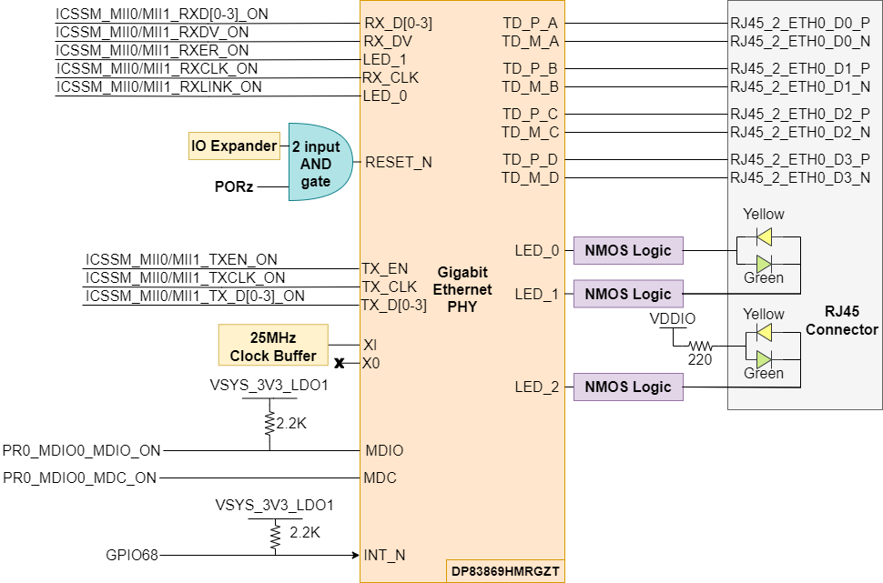
The AM263Px Control Card uses one port of RGMII signals and the PRU0 core of the PRU-ICSS or the PRU1 core of the PRU-ICSS to be connected to a 48pin ethernet PHY (DP83869HMRGZT), depending on how the signals are routed (see Section 2.11.2.1). The PHY is configured to advertise 1 Gbit operation if connected to the PRU0 core. If connected to the PRU1 core, the PHY is configured for 10/100 Mbit operation. The ethernet data signals of the PHY are terminated to an RJ45 Connector. LEDs are used to indicate link status and activity.
 Figure 2-21 Control Card On Board Ethernet
PHY
Figure 2-21 Control Card On Board Ethernet
PHYThe Ethernet PHY requires three separate power sources. There are two dedicated LDO for the 1.1V and 2.5V supplies for the Ethernet PHY. The VDDIO supply for the ethernet PHY is supplied through a load switch (U16) that is enabled once the 2.5V power good signal is driven high.
The RGMII2 port of the CPSW signals are internally muxed on the same balls as the PRU-ICSS ethernet signals. To use RGMII2, the balls must be set to the appropriate mux mode for RGMII2.
There are series termination resistors on the transmit and receive clock signals located near the AM263Px SoC.
The MDIO and Interrupt signals from the SoC to the PHY require 2.2KΩ pull up resistors to the I/O supply voltage for proper operation. The interrupt signal is driven by a GPIO signal that is mapped from the AM263Px SoC.
The reset signal for the Ethernet PHY is driven by a 2-input AND gate. The AND inputs of the gate are a GPIO signal that is generated by the IO Expander and PORz.
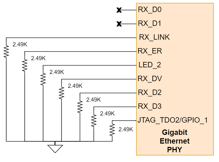
The Ethernet PHY uses many functional pins as strap option to place the device into specific modes of operation.
 Figure 2-22 Industrial Ethernet PHY
Strapping Resistors
Figure 2-22 Industrial Ethernet PHY
Strapping Resistors| Functional Pin | Default Mode | Mode in CC | Function |
|---|---|---|---|
| RX_D0 | 0 | 0 | PHY address: 0000 |
| RX_D1 | 0 | 0 | |
| JTAG_TDO/GPIO_1 | 0 | 0 | RGMII to Copper |
| RX_D3 | 0 | 0 | |
| RX_D2 | 0 | 0 | |
| LED_0 | 0 | 0 | Auto-negotiation, 1000/100/10 advertised, auto MDI-X |
| RX_ER | 0 | 0 | |
| LED_2 | 0 | 0 | |
| RX_DV | 0 | 0 | Port Mirroring Disabled |