SPRUJ86C October 2023 – August 2024 AM263P2 , AM263P4 , AM263P4-Q1
- 1
- Description
- Features
- 4
- 1Evaluation Module Overview
-
2Hardware
- 2.1 Component Identification
- 2.2 Power Requirements
- 2.3 Functional Block Diagram
- 2.4 Reset
- 2.5 Clock
- 2.6 Boot Mode Selection
- 2.7 JTAG Path Selection
- 2.8 Header Information
- 2.9 GPIO Mapping
- 2.10 Push Buttons
- 2.11 Interfaces
- 2.12 HSEC Pinout and Pinmux Mapping
- 3Hardware Design Files
- 4Additional Information
- 5Related Documentation
- 6References
- 7Revision History
- 8Revision History
2.4 Reset
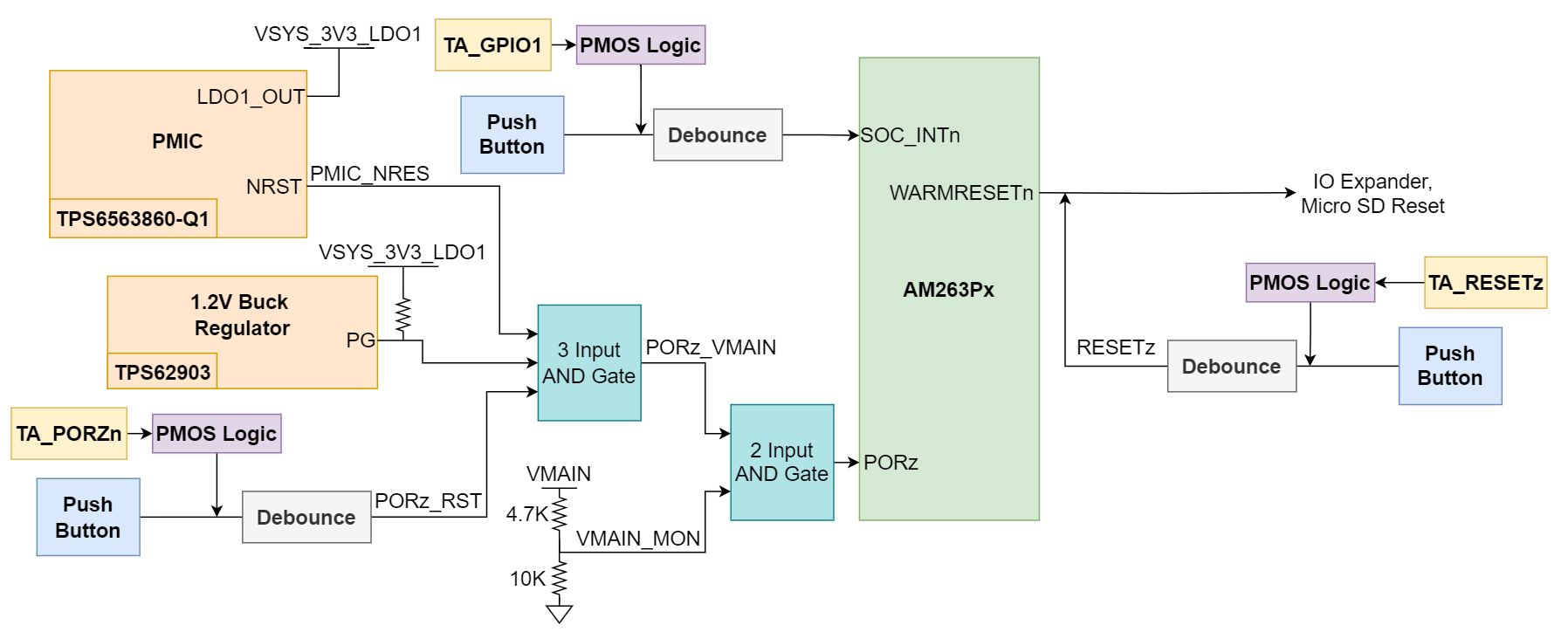
Figure 2-10 shows the reset architecture of the AM263Px Control Card.
 Figure 2-10 Reset Architecture
The AM263Px SoC has the following resets:
- PORz is the Power-On-Reset for the MAIN Domain.
- WARMRESETn is the Warm Reset to MAIN Domain.
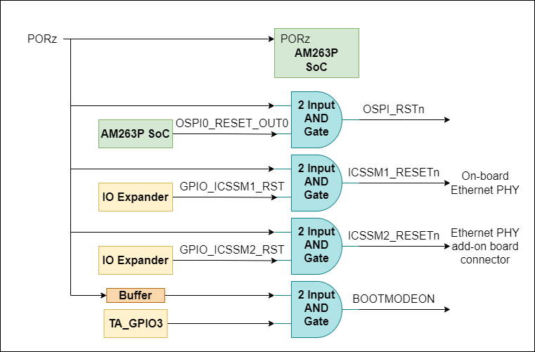
 Figure 2-11 PORz Reset Signal Tree
The PORz signal is driven by a 3-input AND gate that generates a power on reset for the MAIN domain when:
- The PMIC drives the NRES, MCU Reset output signal low.
- The 1.2V buck regulator outputs a low signal for the power good signal.
- The user push button (SW10) is pressed.
- The Test Automation Header outputs a logic LOW signal (TA_PORZn) to a P-Channel MOSFET gate which causes V_GS of the PMOS to be less than zero and so the PORz signal connects to the PMOS drain which is tied directly to ground.
The PORz signal is tied to:
- AM263Px SoC PORz input
- OSPI Flash Reset
- On-board Gigabit Ethernet PHY reset
- Ethernet add-on board connector
- BOOTMODE buffer output enable
- High-Speed Edge Connector (HSEC)
 Figure 2-12 WARMRESETn Reset Signal
Tree
Figure 2-12 WARMRESETn Reset Signal
TreeThe WARMRESETn signal creates a warm reset to the MAIN domain when:
- The user push button (SW12) is pressed.
- The Test Automation Header outputs a logic LOW signal (TA_RESETz) to a P-Channel MOSFET gate which causes V_GS of the PMOS to be less than zero and so the RESETz signal connects to the PMOS drain which is tied directly to ground.
The WARMRESETn signal is tied to:
- AM263Px SoC WARMRESETN output
- RESETz signal created from push button + PMOS logic
- IO Expander reset
- Micro SD reset
- HSEC
The AM263Px Control Card also has an external interrupt to the SoC, INTn, that occurs when:
- The user push button (SW11) is pressed.
- The Test Automation Header outputs a logic LOW signal (TA_GPIO1) to a P-Channel MOSFET gate which causes V_GS of the PMOS to be less than zero and so the INTn signal connects to the PMOS drain which is tied directly to ground.