SPRUJ86C October 2023 – August 2024 AM263P2 , AM263P4 , AM263P4-Q1
- 1
- Description
- Features
- 4
- 1Evaluation Module Overview
-
2Hardware
- 2.1 Component Identification
- 2.2 Power Requirements
- 2.3 Functional Block Diagram
- 2.4 Reset
- 2.5 Clock
- 2.6 Boot Mode Selection
- 2.7 JTAG Path Selection
- 2.8 Header Information
- 2.9 GPIO Mapping
- 2.10 Push Buttons
- 2.11 Interfaces
- 2.12 HSEC Pinout and Pinmux Mapping
- 3Hardware Design Files
- 4Additional Information
- 5Related Documentation
- 6References
- 7Revision History
- 8Revision History
2.11.1.1 OSPI/QSPI
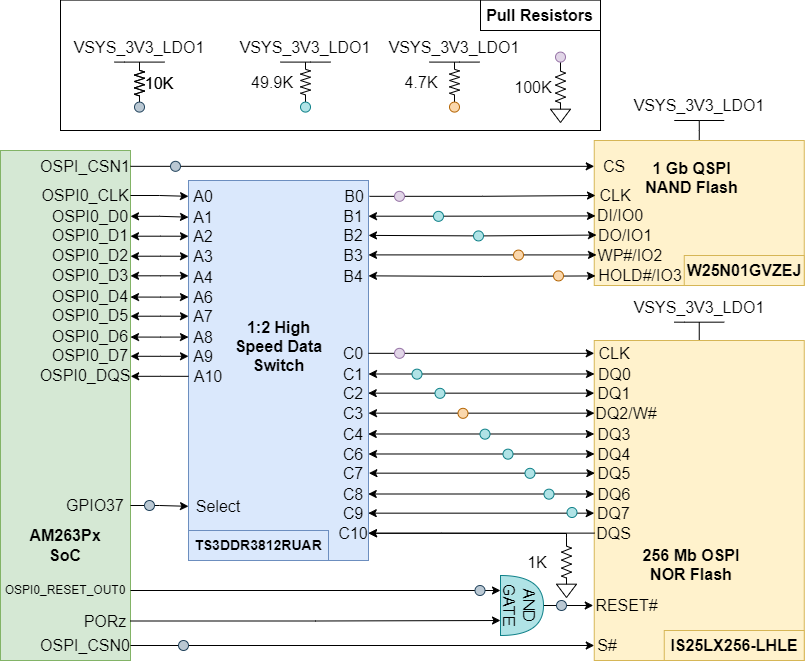
The AM263Px Control Card has a 1Gbit QSPI NAND flash memory device (W25N01GVZEAG), which is connected to the QSPI0 interface of the AM263Px SoC. The QSPI supports single data rates with memory speeds up to 104MHz. The QSPI flash is powered by the 3.3V IO supply (VSYS_3V3_LDO1).
The QSPI0_D0/D1 signals are also used for BOOTMODE control logic. There are 10kΩ resistors used to isolate the BOOTMODE control logic after the value is latched.
The AM263Px Control Card also has a 256Mbit OSPI NOR flash memory device (IS25LX256-LHLE), which is connected to the OSPI0 interface of the AM263Px SoC.
There is a high speed data switch that controls the routing of the memory data signals between the two flash memories. GPIO37 from the AM263Px SoC is used to drive the select line of the high-speed data switch. There is a pull-up resistor on the select line and therefore the OSPI memory device is selected by default.
 Figure 2-18 OSPI/QSPI Interface
| Select | Condition | Mux Function |
|---|---|---|
| HIGH | OSPI NOR flash selected | A→B port |
| LOW | QSPI NAND flash selected | A→C port |