SPRUJ90B March   2023  – February 2024


  1.   1
  2.   F28P650DK9 controlCARD Information Guide
  3.   Trademarks
  4. 1Introduction
  5. 2Hardware Quick Setup Guide
    1. 2.1 Configuration 1: Standalone
    2. 2.2 Configuration 2: External 5V Supply
  6. 3Errata
    1. 3.1 Warnings, Notes, and Errata
    2. 3.2 Warnings About Specific controlCARD Revisions
  7. 4Getting Familiar with the controlCARD
    1. 4.1 F28P65X controlCARD Features
    2. 4.2 Assumed Operating Conditions
      1. 4.2.1 External Power Supply or Accessory Requirements
    3. 4.3 Using the controlCARD
      1. 4.3.1 Clocking Configuration
    4. 4.4 Experimentation Software
  8. 5Special Notes
    1. 5.1 XDS110 Emulator and SCI (UART) Connectivity
    2. 5.2 Evaluation of the Analog-to-Digital Converters (ADCs)
  9. 6Hardware References
  10. 7Revision History

Clocking Configuration

The Clocking tree on this controlCARD is configurable. Both a 20MHz clock source and a 25MHz (default) clock source can be provided to the F28P650DK9 device. To change this configuration, the R75 0Ω resistor must be de-soldered and moved to the R70 location.
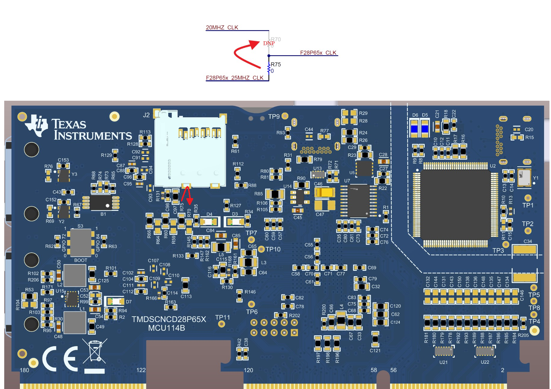
GUID-20230427-SS0I-1CQW-W90S-ZQZCBCCRM2P8-low.png Figure 4-1 Changing the Clock Source From 25MHz to 20MHz