SPRUJ93 august 2023
- 1
- Description
- Features
- 4
- 1Evaluation Module Overview
-
2Hardware
- 2.1 Functional Block Diagram
- 2.2 Component Identification
- 2.3 Power Requirements
- 2.4 Reset
- 2.5 Clock
- 2.6 Boot Mode Selection
- 2.7 JTAG Path Selection
- 2.8 Header Information
- 2.9 GPIO Mapping
- 2.10 Push Buttons
- 2.11 Test Points
- 2.12 Interfaces
- 2.13 HSEC Pinout and Pinmux Mapping
- 3Software
- 4Hardware Design Files
- 5Additional Information
- 6References
2.12.2.2 PRU-ICSS
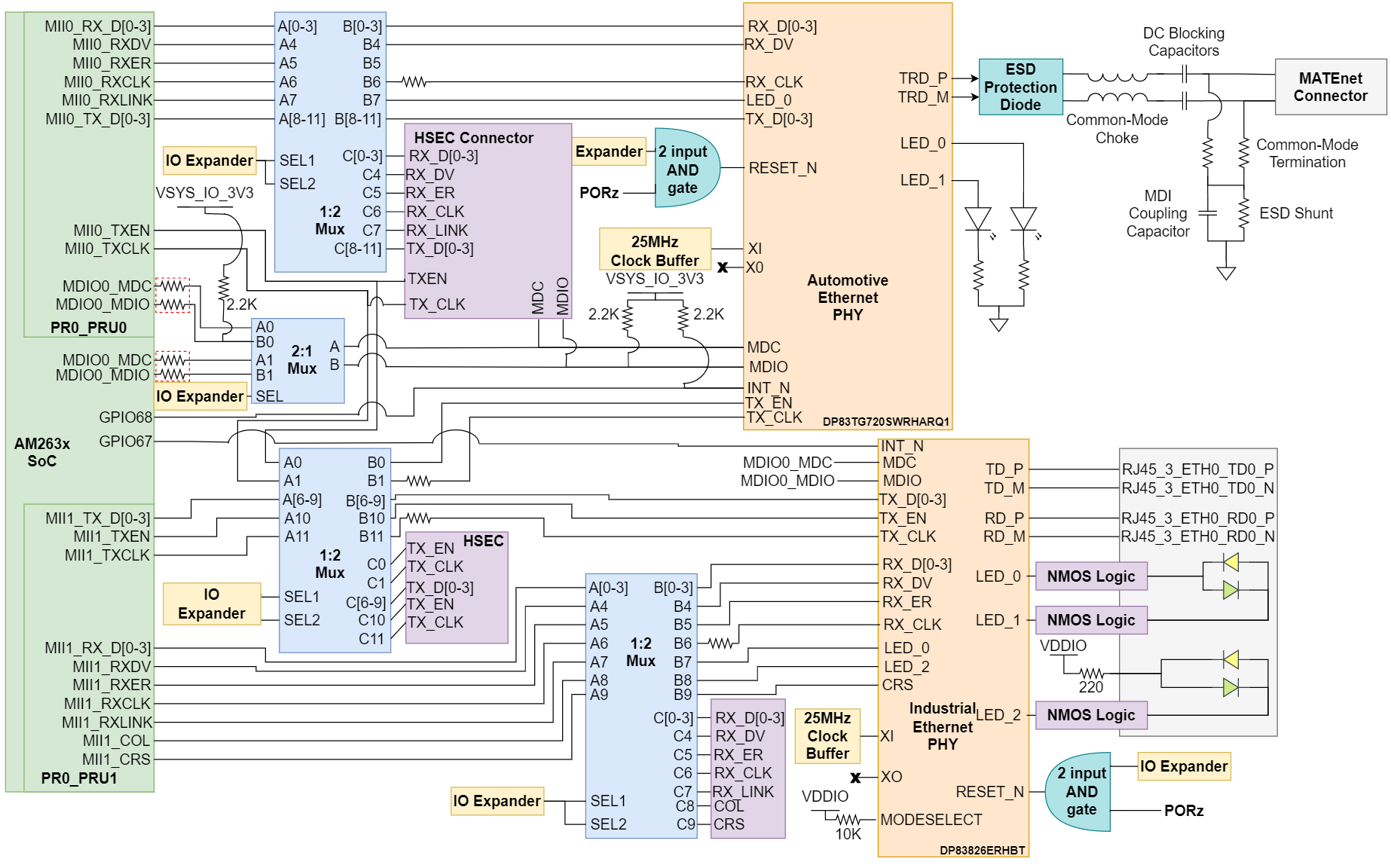
The AM263x Control Card makes use of two on-die programmable real-time unit and industrial communication subsystem's (PRU-ICSS) of the AM263x SoC to interface with two Ethernet PHY transceivers. There is a Automotive Ethernet PHY transceiver (DP83TG720SWRHARQ1) connected to PRU0 of the SoC and an Industrial Ethernet PHY transceiver (DP83826ERHBT) connected to PRU1. The Ethernet data signals of the Automotive Ethernet PHY are terminated to a MATEnet Connector while the Industrial Ethernet PHY data signals are terminated to an RJ45 connector. The MATEnet Connector used on the board supports Gigabit Ethernet by the IEEE 802.3 standard 1000BASE-T1. The RJ45 connector used on the board supports 10/100 (DP83826ERHBT) Mbps connectivity with integrated magnetic and LEDs for link and activity indication.
 Figure 2-20 PRU-ICSS Overview
For the Automotive Ethernet PHY:
- The Ethernet PHY requires three separate power sources. VSYS_3V3A from the PMIC is filtered using two different ferrite beads to supply voltage to VDDIO and VDDA of the Ethernet PHY. There is a dedicated LDO for the 1.0V supply for the Ethernet PHY.
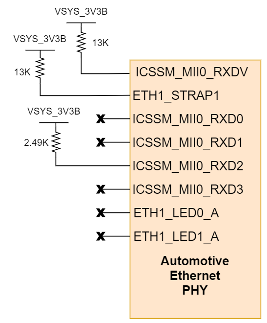
- The Ethernet PHY uses many functional pins as strap options to place the device into a specific mode of operation. Each functional pin has a default mode that is driven by an internal pull resistor.
- There is a 2:1 mux (TMUX154EDGSR) that controls the mapping of MDIO and MDC signals for the ethernet PHY's.
| SEL | Condition | Function |
|---|---|---|
| HIGH | AM263x SoC MDIO0 MDIO/MDC signals selected | A1/B1→A/B port |
| LOW | PRU MDIO/MDC signals selected | A0/B0→ A/B port |
 Figure 2-21 PRU0 ICSS Automotive Ethernet
PHY Strapping Resistors
Figure 2-21 PRU0 ICSS Automotive Ethernet
PHY Strapping Resistors| Functional Pin | Default Mode | Mode in CC | Function |
|---|---|---|---|
| RX_D0 | 0 | 0 | RGMII (Align Mode) |
| RX_D1 | 0 | 0 | |
| RX_D2 | 0 | 1 | |
| RX_CTRL | 0 | 1 | PHY Address: 0x000C |
| STRP_1 | 0 | 1 | |
| LED_0 | 0 | 0 | MS: Peripheral |
| LED_1 | 0 | 0 | AUTO: Autonomous |
For the Industrial Ethernet PHY transceiver:
- The Ethernet PHY requires two separate power sources. VSYS_3V3B from the PMIC is filtered by two separate ferrite beads to be used as the supply for VDDIO and VDDA3V3.
- The Ethernet PHY is set to
ENHANCED mode by pulling the MODESELECT pin up to VSYS_3V3B.
- ENHANCED mode allows the DP83826E to support real-time Ethernet applications in addition to standard Ethernet applications.
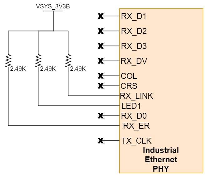
- The Ethernet PHY uses many functional pins as strap options to place the device into a specific mode of operation. Each functional pin has a default mode that is driven by an internal pull resistor
 Figure 2-22 PRU1 ICSS Industrial Ethernet
PHY Strapping Resistors
Figure 2-22 PRU1 ICSS Industrial Ethernet
PHY Strapping Resistors| Functional Pin | Default Mode | Mode in CC | Function |
|---|---|---|---|
| RX_D0 | 1 | 1 | auto-negotiation enable |
| LED1 | 1 | 1 | odd nibble detection enable |
| RX_LINK | 0 | 1 | PHY address: 001 |
| CRS | 0 | 0 | |
| COL | 0 | 0 | |
| TX_CLK | 0 | 0 | RMII Controller Mode |
| RX_ER | 0 | 1 | LED1 on pin 31 |
| RX_D3 | 0 | 0 | fast link-drop disable |
| RX_D2 | 0 | 0 | MII MAC mode |
| RX_D1 | 0 | 0 | Auto MDIX enable |
| RX_DV | 0 | 0 | MDIX (applicable only when auto-MIDX is disabled) |
For both Ethernet PHYs:
- There are series termination resistors on the transmit and receive clock signals located near the AM263x SoC.
- The MDIO and Interrupt signals from the SoC to the PHY require 2.2KΩ pull up resistors to the I/O supply voltage for proper operation. The interrupt signal is driven by a GPIO signal that is mapped from the AM263x SoC.
- The reset signal for the Ethernet PHY is driven by a 2-input AND gate. The AND gate's inputs are a GPIO signal that is generated by the IO Expander and PORz.
- A 25 MHz clock is sourced from a four output clock buffer that has a 25 MHz oscillator as an input.
- There are three 1:2 muxes (TS3DDR3812RUAR) that control the mapping of ethernet signals from the SoC to either the Ethernet PHY's or the HSEC connector. The select logic for the three muxes is driven by two GPIO signals that are generated by the IO expander.
| Select Signal | Logic Level | Condition | Function |
|---|---|---|---|
| ICSSM1_MUX_SEL | LOW | PRU0 signals mapped to Ethernet PHY | A[n] → B[n] |
| HIGH | PRU0 signals mapped to HSEC | A[n] → C[n] | |
| ICSSM2_MUX_SEL | LOW | PRU1 signals mapped to Ethernet PHY | A[n] → B[n] |
| HIGH | PRU1 signals mapped to HSEC | A[n] → C[n] |