SPRUJ93 august 2023
- 1
- Description
- Features
- 4
- 1Evaluation Module Overview
-
2Hardware
- 2.1 Functional Block Diagram
- 2.2 Component Identification
- 2.3 Power Requirements
- 2.4 Reset
- 2.5 Clock
- 2.6 Boot Mode Selection
- 2.7 JTAG Path Selection
- 2.8 Header Information
- 2.9 GPIO Mapping
- 2.10 Push Buttons
- 2.11 Test Points
- 2.12 Interfaces
- 2.13 HSEC Pinout and Pinmux Mapping
- 3Software
- 4Hardware Design Files
- 5Additional Information
- 6References
2.12.9 JTAG
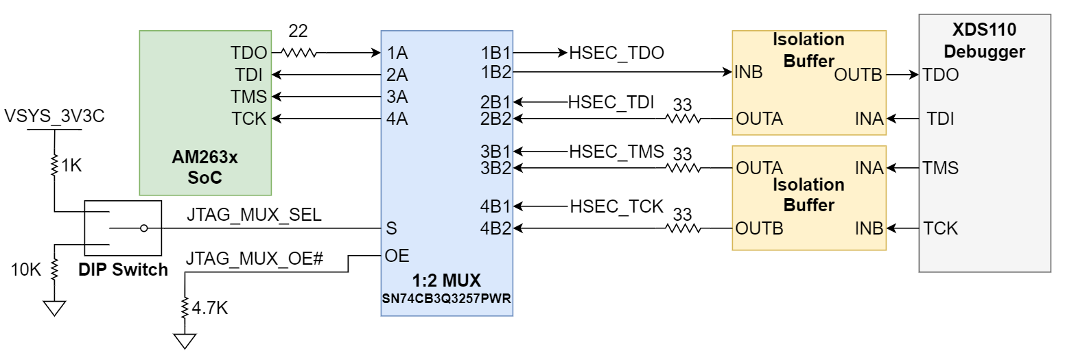
The AM263x Control Card includes an XDS110 class on-board emulator. The control card also has the option to map the JTAG signals from the AM263x SoC to the HSEC connector.
 Figure 2-30 JTAG
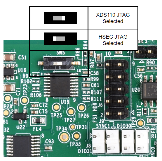
A DIP switch is used to drive the select line of a 1:2 mux (SN74CB3Q3257PWR) that determines the path of the AM263x SoC JTAG signals. Figure 3-31 shows JTAG path selection for either switch position.
 Figure 2-31 JTAG Path Switch
Position
Figure 2-31 JTAG Path Switch
PositionThe Control Card includes all circuitry needed for XDS110 emulation. The emulator uses a USB 2.0 micro-B connector to interface the USB 2.0 signals that are created from the UART-USB bridge. The VBUS power from the connector is used to power the emulation circuit so that the connection to the emulator is not lost when power to the Control Card is removed.
The XDS110 controls two power status LED's. For more information refer to Section 2.3.2.