SPRUJF4A October   2024  – December 2024


  1.   1
  2.   Description
  3.   Features
  4.   Applications
  5.   5
  6. 1Evaluation Module Overview
    1. 1.1 Introduction
    2. 1.2 Kit Contents
    3. 1.3 Specification
    4. 1.4 Device Information
    5.     General Texas Instruments High Voltage Evaluation (TI HV EVM) User Safety Guidelines
  7. 2Hardware
    1. 2.1 Hardware Description
      1. 2.1.1 Auxiliary Power Supply
      2. 2.1.2 DC Link Voltage Sensing
      3. 2.1.3 Motor Phase Voltage Sensing
      4. 2.1.4 Motor Phase Current Sensing
        1. 2.1.4.1 Three-Shunt Current Sensing
        2. 2.1.4.2 Single-Shunt Current Sensing
      5. 2.1.5 External Overcurrent Protection
      6. 2.1.6 Internal Overcurrent Protection for TMS320F2800F137
    2. 2.2 Getting Started Hardware
      1. 2.2.1 Test Conditions and Equipment
      2. 2.2.2 Test Setup
  8. 3Motor Control Software
    1. 3.1 Three-Phase PMSM Drive System Design Theory
      1. 3.1.1 Field-Oriented Control of PMSM
        1. 3.1.1.1 Space Vector Definition and Projection
          1. 3.1.1.1.1 ( a ,   b ) ⇒ ( α , β ) Clarke Transformation
          2. 3.1.1.1.2 ( α , β ) ⇒ ( d ,   q ) Park Transformation
        2. 3.1.1.2 Basic Scheme of FOC for AC Motor
        3. 3.1.1.3 Rotor Flux Position
      2. 3.1.2 Sensorless Control of PM Synchronous Motor
        1. 3.1.2.1 Enhanced Sliding Mode Observer With Phase-Locked Loop
          1. 3.1.2.1.1 Mathematical Model and FOC Structure of an IPMSM
          2. 3.1.2.1.2 Design of ESMO for the IPMS
            1. 3.1.2.1.2.1 Rotor Position and Speed Estimation With PLL
      3. 3.1.3 Field Weakening (FW) and Maximum Torque Per Ampere (MTPA) Control
    2. 3.2 Getting Started Software
      1. 3.2.1 GUI
      2. 3.2.2 Download and Install C2000 Software
      3. 3.2.3 Using the Software
      4. 3.2.4 Project Structure
  9. 4Test Procedure and Results
    1. 4.1 Build Level 1: CPU and Board Setup
    2. 4.2 Build Level 2: Open-Loop Check With ADC Feedback
    3. 4.3 Build Level 3: Closed Current Loop Check
    4. 4.4 Build Level 4: Full Motor Drive Control
    5. 4.5 Test Procedure
      1. 4.5.1 Startup
      2. 4.5.2 Build and Load Project
      3. 4.5.3 Setup Debug Environment Windows
      4. 4.5.4 Run the Code
        1. 4.5.4.1 Build Level 1 Test Procedure
        2. 4.5.4.2 Build Level 2 Test Procedure
        3. 4.5.4.3 Build Level 3 Test Procedure
        4. 4.5.4.4 Build Level 4 Test Procedure
          1. 4.5.4.4.1 Tuning Motor Drive FOC Parameters
          2. 4.5.4.4.2 Tuning Field Weakening and MTPA Control Parameters
          3. 4.5.4.4.3 Tuning Current Sensing Parameters
    6. 4.6 Performance Data and Results
      1. 4.6.1 Load and Thermal Test
      2. 4.6.2 Overcurrent Protection by External Comparator
      3. 4.6.3 Overcurrent Protection by Internal CMPSS
  10. 5Hardware Design Files
    1. 5.1 Schematics
    2. 5.2 PCB Layouts
    3. 5.3 Bill of Materials (BOM)
  11. 6Additional Information
    1. 6.1 Known Hardware or Software Issues
    2. 6.2 Trademarks
    3. 6.3 Terminology
  12. 7References
  13. 8Revision History

Test Setup

  1. Optionally, use 4 included screws to attach the board to the standoffs. Each corner of the TIEVM-MTR-HVINV has a circular hole for this purpose.

  2. If not already connected, connect the daughterboard to the top of the motherboard. The 2-row header of the motherboard (J15) should align with the 2-row connector of the daughterboard (J3).
  3. Key pin 8 of daughterboard connector J3 should be clipped if it is not already done.
  4. Observe the bottom of the XDS110ISO-EVM and locate the key pin. Connect the XDS110ISO-EVM to daughterboard connector J3, such that the key pins of each board are aligned.
  5. Verify the desired state of the daughterboard boot mode switch (S1).
  6. Connect motor wires to J10.
    1. For the Estun EMJ-04APB22, the following is an example image showing how it may be connected:
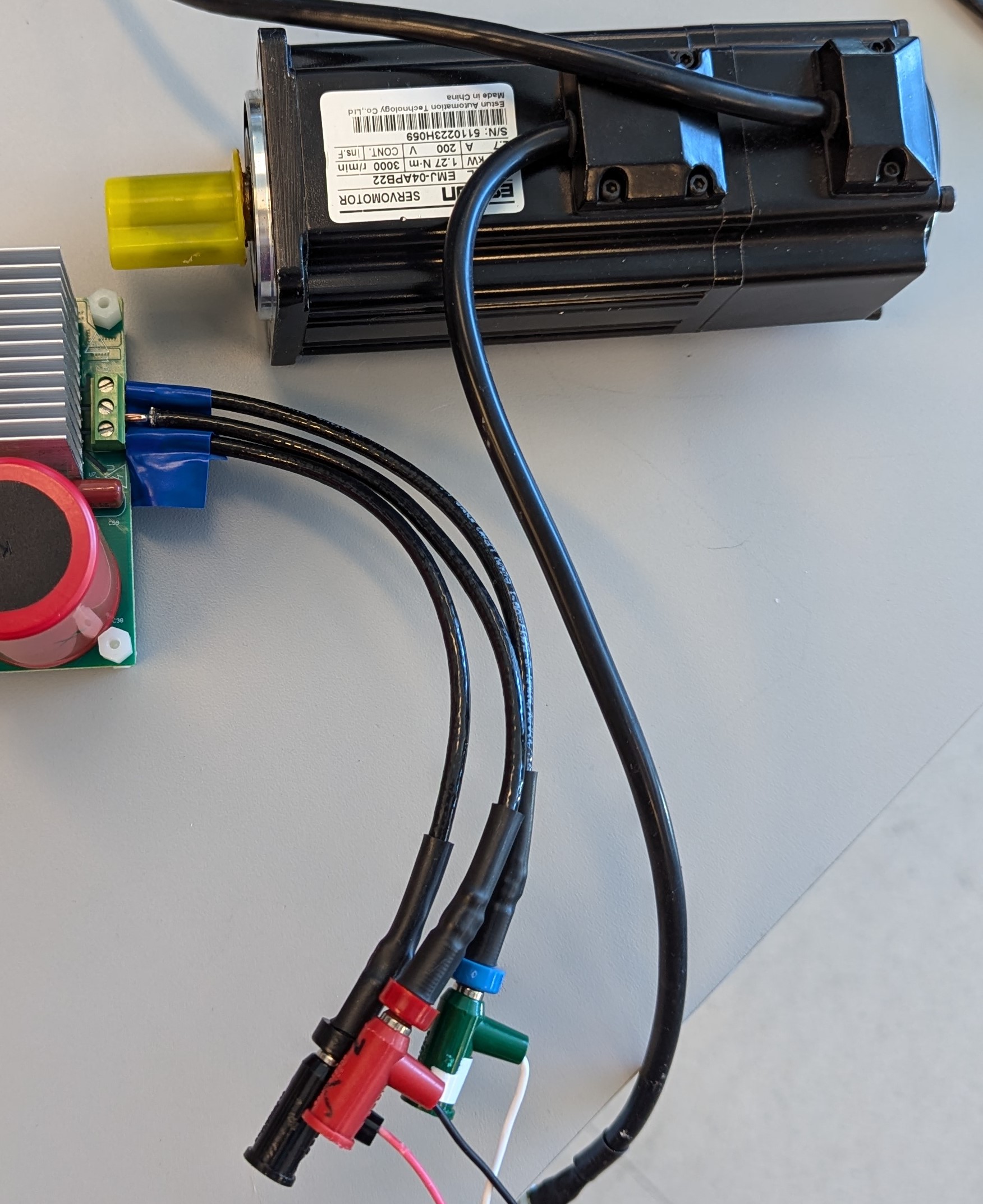
    TIEVM-MTR-HVINV

  7. Connect measurement equipment, such as multimeter, oscilloscope probes, and so forth, to probe or analyze various signals and parameters. Available test points can be viewed in the board schematic (TPx).
  8. Power on the board with isolated AC or DC power supply to the J5 ACL, ACN, and Earth connector.
    1. The maximum output of the AC power supply is 265-VAC, 50/60Hz.
    2. The maximum output of the DC power supply is 380-VDC.

The following options are also available.

  • Daughterboard connector J4 pins 4 through 7 are available as SPI signals, should the user require external SPI. When doing so, the XDS110ISO-EVM on-board DAC is not available. This connection can be used by either:
    • Connecting directly to the SPI signals on daughterboard connector J4. This connection is NOT isolated, and an external isolator must be used.
    • Connecting to isolated UART interface J14, which may not be available on certain board revisions.
  • If using this connection, depopulate daughterboard resistor R8 to ensure that the XDS110ISO-EVM on-board DAC does not interfere with the SPI peripheral-to-controller signals.
  • The default board state utilizes three-phase current sensing. Should single-phase be required, refer to Section 2.1.4.2.