SSZTAS5 october 2016
Generating DC currents of arbitrary magnitude is a simple and straightforward process using operational amplifier feedback and a voltage reference. To this point, we have addressed several external opamp architectures for realizing individual or networks of current sources and sinks. In this final installment of the series, we will address an architecture which utilizes feedback from within the voltage reference itself. Let’s begin by considering the voltage reference’s symbol and its actual functional block diagram as displayed in Figure 1 below.
 Figure 1 Voltage Reference and Its
Functional Block Diagram
Figure 1 Voltage Reference and Its
Functional Block DiagramWe have borrowed the symbol for the Zener diode because that’s essentially how the voltage reference behaves; however, this behavior is achieved through clever design rather than simple device physics alone. Consider the self-referenced (cathode-reference-tied) configuration that was utilized in previous posts and shown in Figure 2 below.
 Figure 2 Voltage Reference Typical
Operation
Figure 2 Voltage Reference Typical
OperationSo, what can we say about this set up? First of all, we can greatly simplify and define the situation with all the currents in Figure 2 as shown in Equation 1.
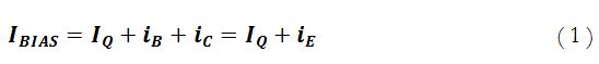
That is, IBIAS is the summation of the opamp quiescent current, IQ, and the emitter current, iE, of the bipolar junction transistor (BJT). Equation 2 further simplifies this by acknowledging that the opamp quiescent current will be negligible compared to the emitter current during normal operation.

Equations 3 and 4 define the emitter current beginning with the diode equation for the base-emitter junction and assuming forward bias operation with nominal ideality factor.
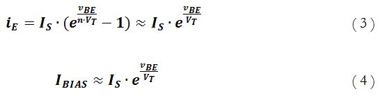
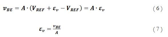
As indicated by Equation 4 above, there must be some base-emitter voltage present to maintain IBIAS. This of course implies that there is a non-zero difference between vref and VREF in Figure 2; we will account for this by defining vref in Equation 5 in terms of VREF and a small perturbation voltage, εv.
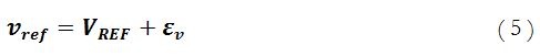
We can now define εv in terms of the base-emitter voltage and opamp gain as shown in Equations 6 and 7.
Clearly εv drops to zero in the ideal opamp case; however, let’s consider some very conservative values. Equation 8 below solves Equation 7 assuming the vBE required to maintain IBIAS is 0.5V and the gain of the opamp is a mediocre 104.
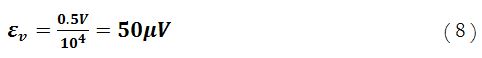
For a 1.25V voltage reference, this represents an error of some four thousandths of a percent or 40ppm—that is, such an error can be safely regarded as negligible.
Now consider what happens to εv when we increase the input voltage, and therefore IBIAS; specifically, suppose we double IBIAS from some arbitrary operating point as illustrated by Equations 9 and 10.
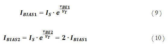
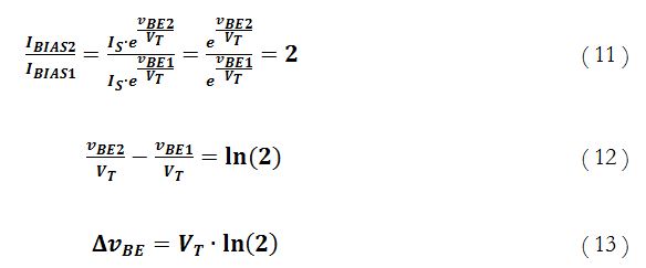
The change in VBE required to support doubling IBIAS can now be derived by dividing Equation 10 by Equation 9 and simplifying terms as follows in Equations 11 through 13.
Finally, we can derive an equation for the change in εv required to support doubling IBIAS as shown in Equations 14 and 15.
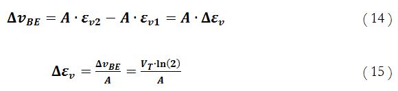
Substituting in the room temperature value of the thermal voltage, VT, and assuming (again) the mediocre opamp gain of 104 we can solve Equation 15 for a conservative value of Δεv required for doubling IBIAS, resulting in Equation 16 below.
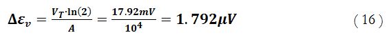
In this case, every time IBIAS is doubled the voltage at vref increases by only 1.792μV. It is this multiplication of opamp gain with the exponential IV characteristic of the base-emitter diode which mimics Zener breakdown behavior.
Connecting the voltage reference differently we can leverage its internal opamp to generate a simple current sink as shown in Figure 3 below.
 Figure 3 Simple Voltage Reference
Derived Current Sink
Figure 3 Simple Voltage Reference
Derived Current SinkTo visualize what’s going on here, consider the functional diagram inserted in place of the symbol as shown in Figure 4 below.
 Figure 4 Simple Current Sink Functional
Diagram
Figure 4 Simple Current Sink Functional
DiagramNotice that the VIN, RBIAS, and BJT circuit essentially acts as an inverting output stage for the opamp. Therefore, we can collapse the total combination into a new opamp symbol with a new gain, AT, and reversed input polarity as shown below in Figure 5.
 Figure 5 Simple Current Sink Functional
Diagram and Equivalent Circuit
Figure 5 Simple Current Sink Functional
Diagram and Equivalent CircuitThus, we have arrived at the same current sink circuit discussed in the first post in this series.
Throughout this series we have investigated the important topic of generating current references from voltage references. The first post covers precision, single sources and sinks of arbitrary magnitude (which can, of course, be used to implement bias networks); the second and third posts discuss a method by which bias networks might be derived with a single feedback device if a tradeoff of precision and component count is workable; and finally, this post discusses a greatly simplified method of implementing the current sink (specifically) discussed in the first post. The architectures discussed throughout this series are a handy addition to any design toolbox, and Texas Instruments has a wide variety of voltage references which can be used to realize these designs.