SSZTBU7 december 2015
To an end user, turning on an electronic device is simple; all it takes is the push of a button. It takes a lot of effort to create a smooth power-up experience, however. Turning a system on too quickly could lead to a power-supply failure via a large, uncontrolled inrush current spike. For microprocessor or FPGA based applications, proper operation requires specific power rail sequencing requirements. Sometimes it is best to wait for certain subsystems to power up before enabling downstream circuitry. Using load switches to manage device power sequencing can facilitate a smooth power-on experience for the end user.
In most systems, capacitors placed throughout a design ensure that there are no supply-rail voltage drops. When initially applying power, charging these capacitors can result in an inrush current that can exceed the maximum current ratings of downstream circuitry. If left unaddressed, this can cause voltage rails to fall out of regulation, resulting in the system entering an undesired state. Unchecked inrush current can also damage board connectors and circuit board traces by exceeding their current-carrying capabilities. To manage inrush current, the voltage applied to the capacitive loads needs to have a controlled rise time. All Texas Instruments load switches have an integrated soft start, with some devices even offering an adjustable rise time for varying capacitive loads. Figure 1 shows an illustration representing this integrated soft start.
 Figure 1 A load switch providing a
controlled rise time to a system load
Figure 1 A load switch providing a
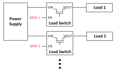
controlled rise time to a system loadPutting a load switch between the power supply and a capacitive load can drastically reduce the inrush current from turning on/enabling the load. Many processors and FPGAs have very specific power-sequencing requirements and a specific order in which the power rails need to turn on. Load switches facilitate power-sequencing requirements, allowing for point-of-load control for each power rail. Powering each rail on then becomes as easy as sending the correct GPIO signal to the correct load switch. Figure 2 illustrates this concept.
 Figure 2 Power sequencing using
separate GPIOs for each load
Figure 2 Power sequencing using
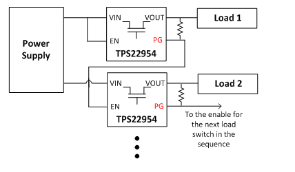
separate GPIOs for each loadSome load switches even have a power-good (PG) signal that indicates when the output has fully turned on. By tying the PG signal to the enable of the next load switch in the sequence, power sequencing only requires one GPIO signal for all of the power rails. Figure 3 shows this configuration.
 Figure 3 Power sequencing with no GPIO
signals needed
Figure 3 Power sequencing with no GPIO
signals neededLoad switches are also effective for powering down systems. The fall time of a load switch is determined by how quickly the output load can discharge its capacitance. To quicken this discharge and guarantee a 0V state, some load switches have a quick output discharge (QOD) feature that discharges the output to ground through an internal resistance, as shown in Figure 4.
 Figure 4 A load switch with QOD
Whether the system is powering up or powering down, load switches can make timing and sequencing requirements as easy as the push of a button. Visit www.ti.com/loadswitches to find the ideal load switch for your power application.
Additional Resources
Learn more about this topic by downloading these application notes: