SSZTCE0 July 2015
When powering up your buck converter for the first time, wouldn’t it be nice to be confident that it will be stable? This is certainly possible by using a simple simulation model and a few simple calculations to set the error amplifier and power-stage gains.
Figure 1 shows a current-mode (CM) model with the error amplifier, power-stage gain and output filter. The error amplifier looks at the output voltage, compares it to an internal reference voltage, and generates an error signal to the power stage. The power-stage gain block converts the error voltage into output current. Simple voltage-controlled current sources model both gains. Adding a lossless transmission line to the output introduces phase lag, improving accuracy at higher bandwidths (BWs).
 Figure 1 CM Control-loop Model
A 1Vac perturbation is injected into the feedback and propagates to the power-stage filter output, V_loop, to measure the system’s loop gain. Making the feedback connection to the positive input of the error amplifier rather than the negative eliminates phase shift. This makes the power supply’s phase margin directly readable at V_loop.
You must determine two error-amplifier parameters: DC gain and operational-amplifier (op-amp) BW. Most controller data sheets specify both parameters. To model the op-amp’s open-loop frequency response, first calculate the output impedance (R_ZO) by dividing the open loop gain of 800V/V (or 58dB) by its transconductance of 92µA/V. This gives an output impedance of 8.7MOhms. Next, calculate the low-frequency pole to set its BW to 2.7MHz, as specified in the data sheet. A pole at 2.7MHz/800 or 3.4kHz is required. Using this pole frequency and the output impedance of 8.7MOhms results in an output capacitance of 5.4pF. Components R2, C1 and C2 provide the external compensation necessary to stabilize the power supply.
I set the power-stage block’s gain to 10A/V based on the data sheet. With CM control, the peak current follows the error signal, turning the inductor into a current source and eliminating it from the model. The output-filter component values must be accurate. They affect the filter pole and zero frequencies, which affect the converter BW and the resulting phase response. Be sure to de-rate the ceramic output capacitor’s capacitance for DC bias, which can often be far less than the stated value. An aluminum capacitor’s equivalent series resistance (ESR) can increase more than tenfold when operated cold, so be sure to verify stability using the highest expected ESR.
The transmission line introduces phase lag, which improves accuracy at higher frequencies. This phase lag is a result of propagation delay and relates to the time the converter actually takes to switch from when initially commanded. An average delay time is about one-half the switching period and introduces a 90° phase lag at one-half the switching frequency. For low-BW converters, the effect will be small. However, as the BW approaches one-half the switching frequency, the phase decreases significantly and better matches the actual phase response. Without this in the model, expect the phase-response error to increase above one-tenth the switching frequency.
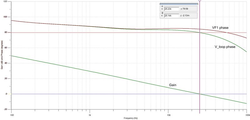
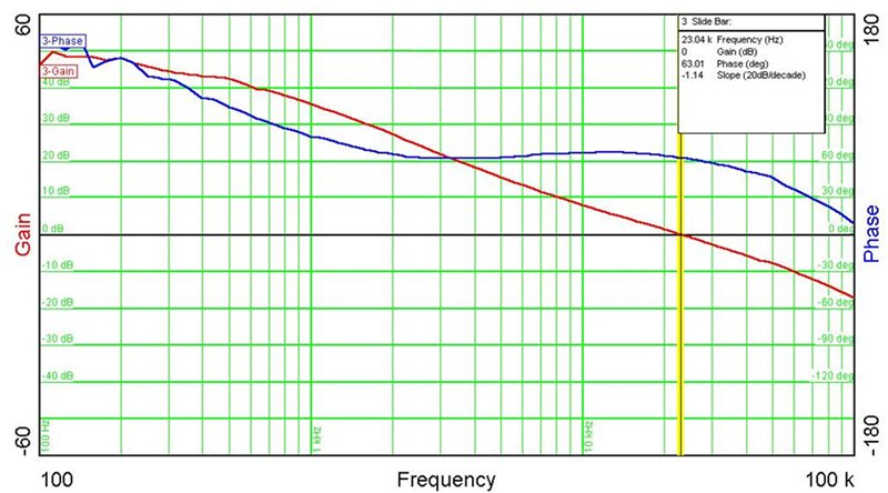
Figure 2 shows the simulated response, while Figure 3 shows the actual measurement. The transmission line decreases the phase at higher frequencies. There is good correlation between the predicted and actual data; however, some error between the two does exist. These differences are likely due to factors such as internal slope compensation and value discrepancies. Figure 2 Simulated CM Model’s Gain and
Phase Margin
 Figure 3 Lab Measurement Shows Good
Correlation
Figure 3 Lab Measurement Shows Good
CorrelationThis model provides a simple method to validate compensation values in CM buck converters with reasonable accuracy. The simulated results can validate stability; reduce test time; and model the effects of second stage L-C filters, long inductive leads and downstream capacitances. It is most useful when setting the initial BW lower for checkout, verifying stability and optimizing for a higher BW.
Additional Resources
- Check out TI’s Power Tips blog series on Power House.
- For more about this topic, see the Power Tips article, “Power Tips: Simulate your buck converter control loop.”