SSZTCT5 april 2015 CSD18540Q5B
Thanks for coming back. If you missed part 1 of this series, I covered the basics of thermal design for three-phase motor drives in power tools; go check it out. In part 2, I’ll cover some general guidelines for a good thermal design
Here are a few important points to consider for good thermal design of a printed circuit board (PCB):
- Provide large copper planes in the PCB. Solder the exposed pad of the device to the copper plane and extend the plane to the edges of the PCB in order to increase the heat-spreading area. With a four-layer board, you can use copper planes in all of the layers to spread the heat, which in turn can give up to 30% improved performance compared to a two-layer board. The larger the PCB area, the higher the heat dissipation due to convection. Provide the copper planes without any breaks so that the heat spreading through the planes will be efficient.
- Lower thermal resistance with multiple vias. Provide as many thermal vias as possible underneath the device case and connect the vias to the copper planes in all the layers. A typical 12mil diameter through-hole via with 0.5oz copper sidewalls has a thermal resistance of 261°C/W. Completely filling the vias with copper can bring down the thermal resistance by as much as half; however, this technology may double the cost of the PCB. A more economical option is to provide 1oz plating on standard 12mil vias, which would add only a 10-20% additional cost. This can help bring the thermal resistance of a single via to 140°C/W.
- Copper thickness. By increasing the copper thickness of the copper planes, more heat transfers laterally, helping to spread heat to the entire PCB. Increasing the thickness of copper increases PCB cost; however, 2oz copper thickness is a good choice for power-tool applications where there is a size constraint on the PCB. By increasing the copper thickness from 1oz to 2oz, you can achieve up to a 25% increase in thermal performance.
Thermal Design with Heat Sink
The small size of power tools limits the PCB size, requiring the addition of a heat sink to meet safe thermal performance. Based on form-factor restrictions, you can add a heat sink to either the top of the device package or directly beneath the exposed pad on the back side of the PCB. Because of the high thermal resistance from the junction to the top side of the device casing, a heat sink will be more effective when connected to the exposed metal pad of the device through the PCB.
The most efficient way of dissipating the generated heat is to connect a heat sink on the bottom side of the PCB where the metal-oxide semiconductor field-effect transistors (MOSFETs) are mounted. This is because 95% of the heat will be dissipated through the bottom side of the device when no heat sink is mounted on the top side.
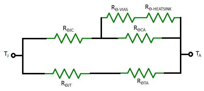
The major challenge will be to reduce the thermal resistance of the PCB between the bottom exposed case of the device and the heat sink. Therefore, the design of thermal vias is a vital component of placing the heat sink on the bottom side. The thermal vias act as thin copper pillars, directly connecting the device’s bottom case to the heat sink. The addition of thermal vias and the heat sink help to reduce the effective thermal resistance from the device’s bottom case to the ambient. Figure 1 shows the thermal equivalent circuit.
 Figure 1 Heat Dissipation Paths of Surface-mount Device (SMD) Packages with a Bottom Heat Sink
Effect of Air Flow
Heat transfer from the surface of the PCB or heat sink to the ambient happens through convection and radiation. With natural airflow, the heat-transfer coefficient from the PCB surface to air is 10 W/m2K. Providing a forced airflow of 100LFM can double the heat transfer coefficient or effectively reduce the thermal resistance from the PCB surface to the ambient by half.
In this blog series, I discussed the basics of thermal design for three-phase motor drives used in power tools. The thermal design of the PCB is a vital part when you design your drive in a small form factor handling high current. To enable your design to handle more power, you can add a heat sink to the bottom side of the PCB where the MOSFETs are mounted.
For more information on a drive design for power-tool applications and design examples, see this TI Designs reference design for a 1kW/36V power stage for a brushless motor in battery-powered garden and power tools. The reference design describes the design of the power stage for driving a three-phase permanent-magnet motor used in power tools. The power stage operates from a 10-cell lithium-ion battery with a voltage range of 36 to 42V. The design uses CSD18540Q5B NexFET™ power MOSFETs featuring a very low drain-to-source resistance (RDS_ON) of 1.8mΩ in a small-outline no-leads (SON) 5 x 6 SMD package, which results in a very small form factor of 57 x 59mm for the power stage.
Additional Resources
- Texas Instruments application report, “Thermal Considerations for Surface Mount Layouts.”
- Texas Instruments data sheet, “CSD18540Q5B 60V N-Channel NexFET Power MOSFETs.”