SWCU192 November 2021 CC1312R7 , CC1352P7 , CC2652P7 , CC2652R7
20.4.4.2.3 Timing Diagrams
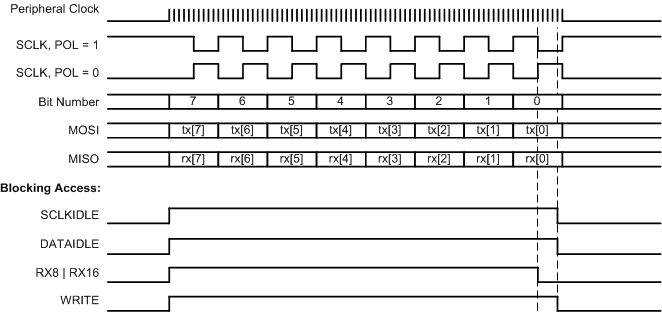
Figure 20-13 and Figure 20-14 show how the configuration of AUX_SPIM:SPIMCFG fields affect the 8-bit data transfer as well as the duration of register access blocking. For the purpose of illustration, the AUX_SPIM:SPIMCFG.DIV is set to 0x4, which gives an SCLK period that is 10 times the peripheral clock period.
In both Figure 20-13 and Figure 20-14, the peripheral clock starts to toggle and blocking begins when the user writes AUX_SPIM:TX8, which indicates the start of transmission. The value of the POL field does not impact the timing of the waveforms; it only sets the IDLE state of SCLK. The value of the PHA field determines the phase of the MOSI and MISO signals with respect to SCLK. As seen in Figure 20-13 and Figure 20-14, this also affects the blocking duration of the AUX_SPIM:SCLKIDLE register access. When PHA = 1, the access completes faster because the SCLK reaches IDLE state earlier.
Set the peripheral clock frequency with AUX_SYSIF:PEROPRATE.SPIM_OP_RATE as follows:
- When then the Sensor Controller owns the peripheral, it must be set to SCE_RATE.
- When the System CPU owns the peripheral, it must be set to BUS_RATE.
 Figure 20-13 SPI Timing Diagram: PHA = 0
 Figure 20-14 SPI Timing Diagram: PHA = 1