SWRA574B October 2017 – February 2020 AWR1243 , AWR2243
2.2.2 Frame (Burst) and Chirp Timing in a Cascaded System
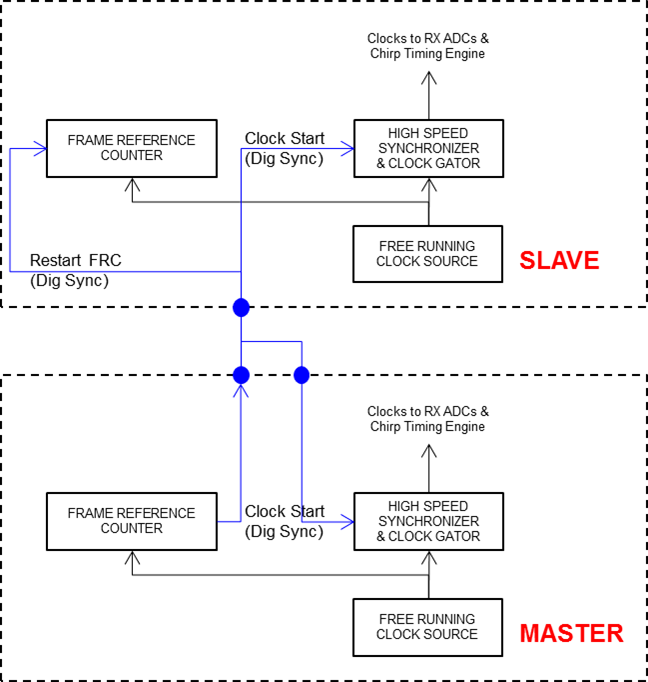
In a cascaded system, the FRC and chirp timing engines of the constituent chips are operated in synchronously. The master chip FRC generates the Dig Sync signal. Dig Sync is routed out of the master and fed to the slaves as well as back to the master to match the skew between master and slave chips. As illustrated in Figure 7 (2 chip cascade example), the Dig Sync is synchronized and used to ungated the clocks to all the RX ADC and chirp timing engines in the master and slaves, thereby ensuring timing alignment across chips. It also ensures that the processor firmware in the master and slaves run in (within 5 ns to 10 ns uncertainty). PCB routing of the Dig Sync signal should be delay matched for best alignment between master and slave chips.
 Figure 6. Frame (Burst) Timing Generation in Two Chip Cascade Example