SWRU612 December   2023 CC3300 , CC3301 , CC3301MOD , CC3351


  1.   1
  2.   Abstract
  3.   Trademarks
  4. 1Introduction
    1. 1.1 Overview
  5. 2Schematic Considerations
    1. 2.1 Schematic Reference Design
    2. 2.2 Power Supply
      1. 2.2.1 Power Input/Output Requirements
      2. 2.2.2 Power-Up Sequence
        1. 2.2.2.1 SOP Modes
    3. 2.3 Clock Source
      1. 2.3.1 Fast Clock
      2. 2.3.2 Slow Clock
        1. 2.3.2.1 Slow Clock Generated Internally
        2. 2.3.2.2 Slow Clock Using an External Oscillator
    4. 2.4 Radio Frequency (RF)
    5. 2.5 Digital Interfaces
      1. 2.5.1 Reset
      2. 2.5.2 Secure Digital Input Output (SDIO)
        1. 2.5.2.1 SDIO Timing Diagram - Default Speed
        2. 2.5.2.2 SDIO Timing Diagram - High Speed
      3. 2.5.3 Serial Peripheral Interface (SPI)
        1. 2.5.3.1 SPI Timing Diagram
      4. 2.5.4 Universal Asynchronous Receiver-Transmitter (UART)
      5. 2.5.5 Serial Wire Debug (SWD)
      6. 2.5.6 Coexistence
  6. 3Layout Considerations
    1. 3.1 Layout Reference Design
      1. 3.1.1 Reference Design Layout
      2. 3.1.2 BP-CC3301 Design Layout
      3. 3.1.3 M2-CC3301 Design Layout
    2. 3.2 IC Thermal Pad
    3. 3.3 Radio Frequency (RF)
    4. 3.4 XTAL
    5. 3.5 Power Supplies
    6. 3.6 SDIO

BP-CC3301 Design Layout

Figure 3-3 is sampled from the BP-CC3301 design files.
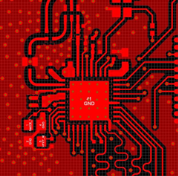
GUID-20231206-SS0I-VC74-S3TK-MQSQDRGSQTNB-low.png Figure 3-3 BP-CC3301 Layout , Top (Layer 1)

Figure 3-4 is sampled from the BP-CC3301 design files.

GUID-20231206-SS0I-ZZNX-V8RK-KCX37XBRGGGX-low.png Figure 3-4 BP-CC3301 Layout, Ground (Layer 2)