SWRU620A April   2024  – December 2024


  1.   1
  2.   Description
  3.   Features
  4.   Applications
  5.   5
  6. 1Evaluation Module Overview
    1. 1.1 Introduction
    2. 1.2 Kit Contents
    3. 1.3 Specification
      1. 1.3.1 Block Diagram
      2. 1.3.2 EVM Mux Block Diagram
    4. 1.4 Device Information
    5. 1.5 IWRL6432AOPEVM Antenna
  7. 2Hardware
    1. 2.1 PCB Material
    2. 2.2 Switches and LEDs
      1. 2.2.1 SOP Configuration
      2. 2.2.2 Switches
    3. 2.3 DC Jack
    4. 2.4 DCA1000 HD Connector
    5. 2.5 CANFD Connector
    6. 2.6 LIN PHY Connection
    7. 2.7 I2C Connections
      1. 2.7.1 EEPROM
      2. 2.7.2 On-Board Sensors
    8. 2.8 XDS110 Interface
    9. 2.9 FTDI Interface
  8. 3Software
    1. 3.1 Software Description
    2. 3.2 Flashing the Board
    3. 3.3 mmWave Out of Box Demo
      1. 3.3.1 IWRL6432AOP Demo Visualization Getting Started
    4. 3.4 DCA1000EVM Mode
  9. 4Hardware Design Files
    1. 4.1 Schematics
    2. 4.2 PCB Layouts
      1. 4.2.1 PCB Storage and Handling Recommendations:
        1. 4.2.1.1 PCB Storage and Handling Recommendations:
        2. 4.2.1.2 Higher Power Demanding Applications
    3. 4.3 Bill of Materials (BOM)
  10. 5Additional Information
    1. 5.1 Trademarks
  11. 6Related Documentation
  12. 7TI E2E Community
  13. 8References
  14. 9Revision History

IWRL6432AOPEVM Antenna

The IWRL6432AOPEVM includes three receiver and two transmitter short range antennas on the package of the chip.Figure 1-3 shows the antenna on package.

Note: There should not be any taller components in the Field Of View (FOV) of the antenna to avoid any multipath reflection. We should also have a keep out area of at least one wavelength (5mm) from either edge of the device.
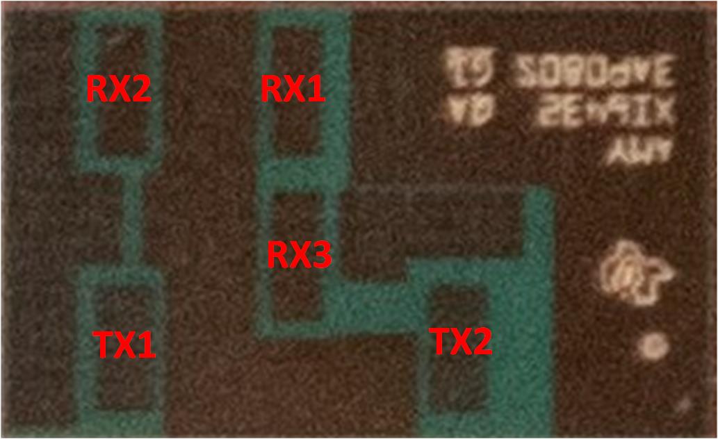
IWRL6432AOPEVM AOP Antennas Figure 1-3 AOP Antennas
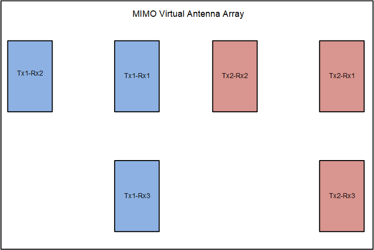
IWRL6432AOPEVM IWRL6432AOP Antenna Placement
                    MIMO Array IWRL6432AOPEVM IWRL6432AOP Antenna Placement
                    MIMO Array Figure 1-4 IWRL6432AOP Antenna Placement MIMO Array