SWRU630 December 2024
- 1
- Description
- Getting Started
- Features
- 1Evaluation Module Overview
-
2Hardware
- 2.1 xWRL6844EVM Antenna
- 2.2 EVM Mux Block Diagram
- 2.3 Switch Settings
- 2.4 Push Button Switches
- 2.5 LEDs
- 2.6 DC Input Jack
- 2.7 USB Connector
- 2.8 DCA1000 HD Connector
- 2.9 BoosterPack Connector for LaunchPad Connectivity
- 2.10 CAN-FD_B Connector
- 2.11 CAN-FD_A Connector
- 2.12 LIN-PHY Connector
- 2.13 I2C Connections
- 2.14 XDS110 Interface
- 2.15 FTDI Interface
- 2.16 DCA1000EVM Mode
- 2.17 PCB Storage and Handling Recommendations:
- 3Software, Development Tools, and Example Code
- 4Hardware Design Files
- 5Additional Information
- 6References
- 7Revision History
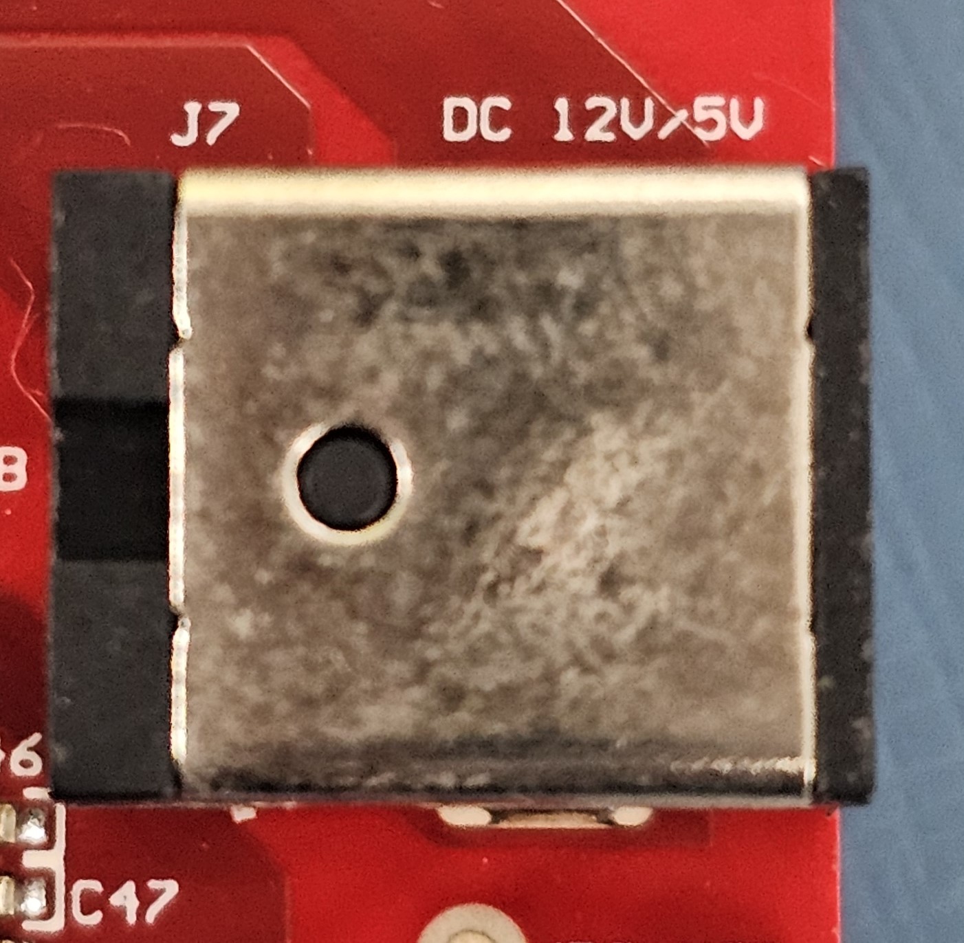
2.6 DC Input Jack
The xWRL6844EVM can be powered-up using the 5V to 12V DC Jack. When DC Jack is connected, the Priority switchover is given to DC-jack's Voltage at the power mux(TPS2121).

Note: After the 5V-12V power supply is provided to the EVM, TI recommends
pressing the NRST switch one time to verify for a reliable boot-up state.
Note: All digital IO pins of the device (except NRESET) are not fail safe.
Therefore, care needs to be taken that the digital
IO pins are not driven externally without the VIO
supply being present to the device.