TIDT199A January   2021  – December 2022


  1.   Description
  2.   Features
  3.   Applications
  4. 1Input Characteristics
    1. 1.1 DC Input Voltage Requirements
  5. 2Testing and Results
    1. 2.1 Efficiency Graphs
    2. 2.2 Standby Power
    3. 2.3 Regulation
    4. 2.4 Current Limit
    5. 2.5 Thermal Images
    6. 2.6 Bode Plots
  6. 3Waveforms
    1. 3.1 Switching
    2. 3.2 Output Voltage Ripple
    3. 3.3 Load Transients
    4. 3.4 Dynamic Response

Switching

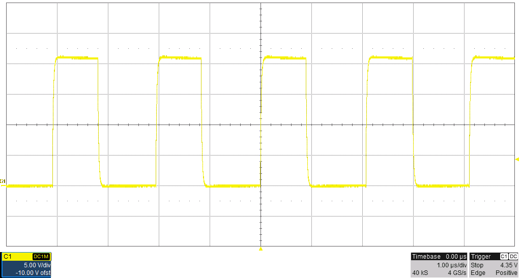
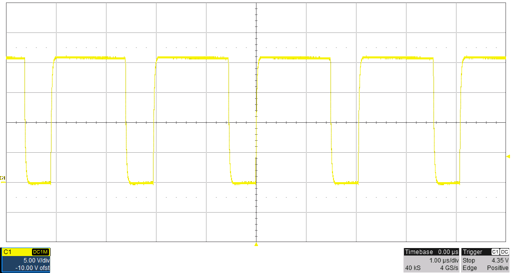
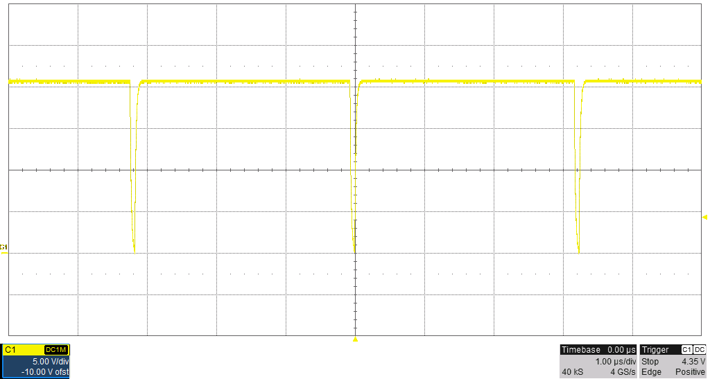
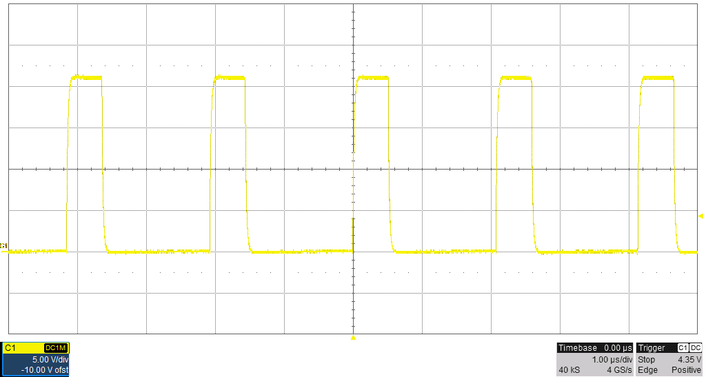
The switching characteristics waveforms are presented in the following images.
GUID-20200930-CA0I-MB9Q-HVXP-CNZXW7QH4HVK-low.pngFigure 3-1 SW to GND, 5-V, 3-A Output
GUID-20200930-CA0I-RFH4-XQCP-LW7HT8HGVRDQ-low.pngFigure 3-2 SW to GND, 9-V, 3-A Output
GUID-20200930-CA0I-WM2D-JNL6-KLBHTWXXLXQW-low.pngFigure 3-3 SW to GND, 15-V, 3-A Output
GUID-20200930-CA0I-KSFD-BDNT-MJTSJH5MKKVB-low.pngFigure 3-4 SW to GND, 20-V, 3.25-A Output