TIDT199A January 2021 – December 2022
2.5 Thermal Images
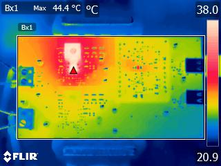
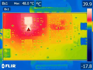
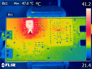
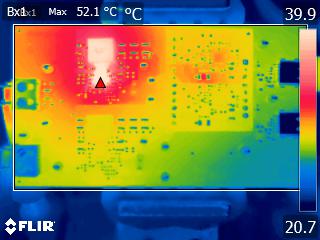
The following thermal images show a top view of the board. The board is placed horizontally during the test. The ambient temperature is 25ºC with no air flow. The output is loaded for 30 minutes. Input voltage is set to 21 V.
 Figure 2-8 5 V, 3 A, Top Side
 Figure 2-10 15 V, 3 A, Top Side
 Figure 2-9 9 V, 3 A, Top Side
 Figure 2-11 20 V, 3.25 A, Top Side